Method of manufacturing light emitting device

a technology of light-emitting devices and manufacturing methods, which is applied in the direction of semiconductor devices, semiconductor/solid-state device details, electrical devices, etc., can solve the problems of difficult formation of reflective resin, inability to arrange the semiconductor elements on the portion proper to reduce,

Active Publication Date: 2017-06-01
NICHIA CORP
View PDF1 Cites 61 Cited by
  • Summary
  • Abstract
  • Description
  • Claims
  • Application Information

AI Technical Summary

Benefits of technology

[0011]With the method of manufacturing a light emitting device according to certain embodiments of the present invention, a resin member that serves as a cover member can be formed in a stable shape.

Problems solved by technology

However, the semiconductor elements may not be able to be arranged on a portion proper to reduce the “sink mark” between the light emitting elements such as in a light emitting device in which the protective elements is not arranged,.
In this case, a reflective resin may be difficult to be formed so as to have a stable height.

Method used


Image

  • Method of manufacturing light emitting device
  • Method of manufacturing light emitting device
  • Method of manufacturing light emitting device

Examples


first embodiment

Structure of Light Emitting Device

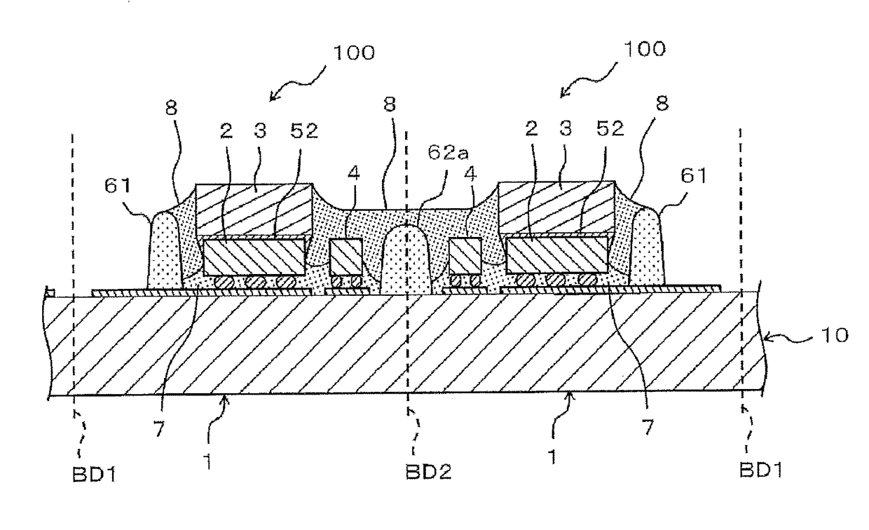
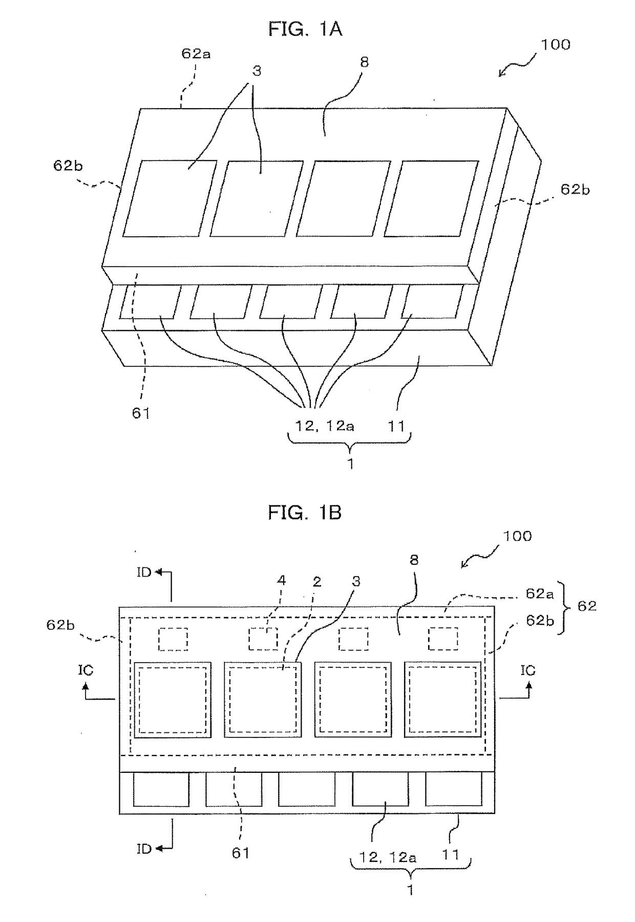
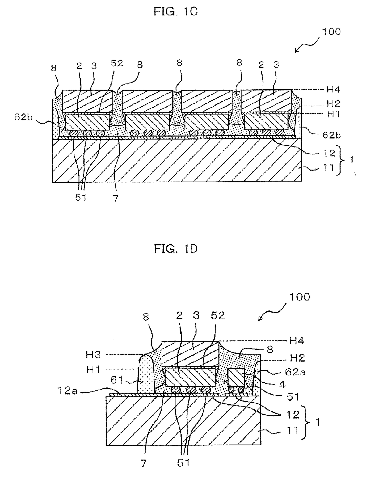
[0042]A structure of a light emitting device according to a first embodiment will be described with reference to FIGS. 1A to 1D.

[0043]FIG. 1A is a schematic perspective view showing a structure of the light emitting device according to the first embodiment. FIG. 1B is a schematic plan view showing the structure of the light emitting device according to the first embodiment. FIG. 1C is a schematic cross-sectional view showing the structure of the light emitting device according to the first embodiment taken along a line IC-IC in FIG. 1B. FIG. 1D is a schematic cross-sectional view showing the structure of the light emitting device according to the first embodiment taken along a line ID-ID in FIG. 1B.

[0044]A light emitting device 100 according to the first embodiment mainly includes: a flat plate-shaped mount substrate 1 having substantially a rectangular shape in a plan view; four light emitting elements 2 mounted on an upper surface of the mount sub...

second embodiment

Configuration of Light Emitting Device

[0122]Next, a light emitting device according to a second embodiment is described below with reference to FIGS. 12A and 12B.

[0123]FIG. 12A is a schematic plan view showing a structure of a light emitting device according to the second embodiment. FIG. 12B is a schematic cross-sectional view showing the structure of the light emitting device according to the second embodiment taken along a line XIIB-XIIB in FIG. 12A.

[0124]The schematic cross-sectional view taken along a line ID-ID in FIG. 12A is substantially the same as the schematic cross-sectional view of the light emitting device 100 shown in FIG. 1D.

[0125]A light emitting device 100B according to the second embodiment is different from the light emitting device 100 according to the first embodiment in that the second protruding member 62b are not arranged at the end portions in the longitudinal direction (i.e., lateral direction in FIG. 12A), an underfill 7B is arranged instead of the underf...


PUM


Abstract

A method of manufacturing a light emitting device includes: mounting light emitting elements on a collective substrate; arranging a first protruding member surrounding the light emitting elements; arranging a second protruding member between the light emitting elements; forming a cover member covering an upper end of the second protruding member, a lateral surface of each of the light emitting elements in a region surrounded by the first protruding member; and singulating the light emitting devices by cutting the cover member, the second protruding member, and the collective substrate at a portion including the second protruding member. The second protruding member is harder than the cover member. An upper end of the second protruding member is located lower than that of the first protruding member but higher than the upper surface of each of the light emitting elements.

Description

CROSS REFERENCE TO RELATED APPLICATION[0001]The present application claims priority to Japanese Patent Application Nos. 2015-233593 filed on Nov. 30, 2015 and 2016-032573 filed on Feb. 24, 2016, the disclosures of all of which are hereby incorporated by reference in their entireties.BACKGROUND[0002]Field[0003]The present invention relates to a method of manufacturing a light emitting device.[0004]Description of the Related Art[0005]Light emitting diodes (LEDs) attracting attention as a next-generation light source has good energy saving effect compared with that in conventional light sources, and can be used for a long time. For this reason, application of light emitting diodes for such as backlights, automobiles, electronic display boards, traffic signal lamps, and general lighting lamps have been spreading industry-wide.[0006]Examples of light emitting devices using LEDs include a light emitting device in which light emitting elements are mounted on a mount substrate having wiring...

Claims


Application Information

Patent Timeline
Patent Type & Authority Applications(United States)
IPC IPC(8): H01L25/16H01L33/60H01L23/00H01L33/54H01L33/58
CPCH01L25/167H01L2933/0033H01L33/58H01L24/96H01L24/97H01L24/73H01L24/26H01L33/60H01L25/0753H01L25/072H01L27/0248H01L29/866H01L2933/005H01L23/24H01L33/62H01L2224/73204H01L2924/1811H01L2224/26155H01L2224/26175H01L2924/12041H01L2924/12035H01L2924/1304H01L2924/1426H01L33/54H01L33/483H01L2933/0058H01L33/0095H01L33/505H01L33/56H01L2224/16227H01L2224/32225H01L2224/73253H01L2224/92225H01L2224/97H01L2924/19105H01L2933/0041H01L2933/0091H01L2224/81H01L2224/83H01L2224/16225H01L2924/00H01L33/52
Inventor OZEKI, KENJIFUKUTA, HIROKI
Owner NICHIA CORP
Why Eureka
Try Eureka