A device controller and method for performing a plurality of write transactions atomically within a nonvolatile data storage device

a non-volatile data storage and device controller technology, applied in the direction of memory adressing/allocation/relocation, multi-programming arrangements, instruments, etc., can solve the problem of not performing an update to the address translation record in the non-volatile data storage devi

Active Publication Date: 2017-06-08
ARM LTD
View PDF6 Cites 21 Cited by
  • Summary
  • Abstract
  • Description
  • Claims
  • Application Information

AI Technical Summary

Benefits of technology

[0015]There are various options as to where within the non-volatile data storage device the intent information is saved. In one embodiment, the non-volatile data storage device comprises a main non-volatile storage unit and a non-volatile cache configured to buffer data prior to writing of that data into the main non-volatile storage unit, and said area of the non-volatile data storage device where the intent information is stored is within said non-volatile cache. In embodiments where non-volatile cache is provided within the data storage device, the storing of the intent information within the non-volatile cache avoids the need to perform any write operations directly within the main non-volatile storage unit merely to store the intent information. This is beneficial, since the intent information is only of transitory interest, to allow determination of situations where the write transactions have not been performed atomically. Normally, it is expected that the write...

Problems solved by technology

However, at this stage, no update to the address translat...

Method used


Image

  • A device controller and method for performing a plurality of write transactions atomically within a nonvolatile data storage device
  • A device controller and method for performing a plurality of write transactions atomically within a nonvolatile data storage device
  • A device controller and method for performing a plurality of write transactions atomically within a nonvolatile data storage device

Examples


Embodiment Construction

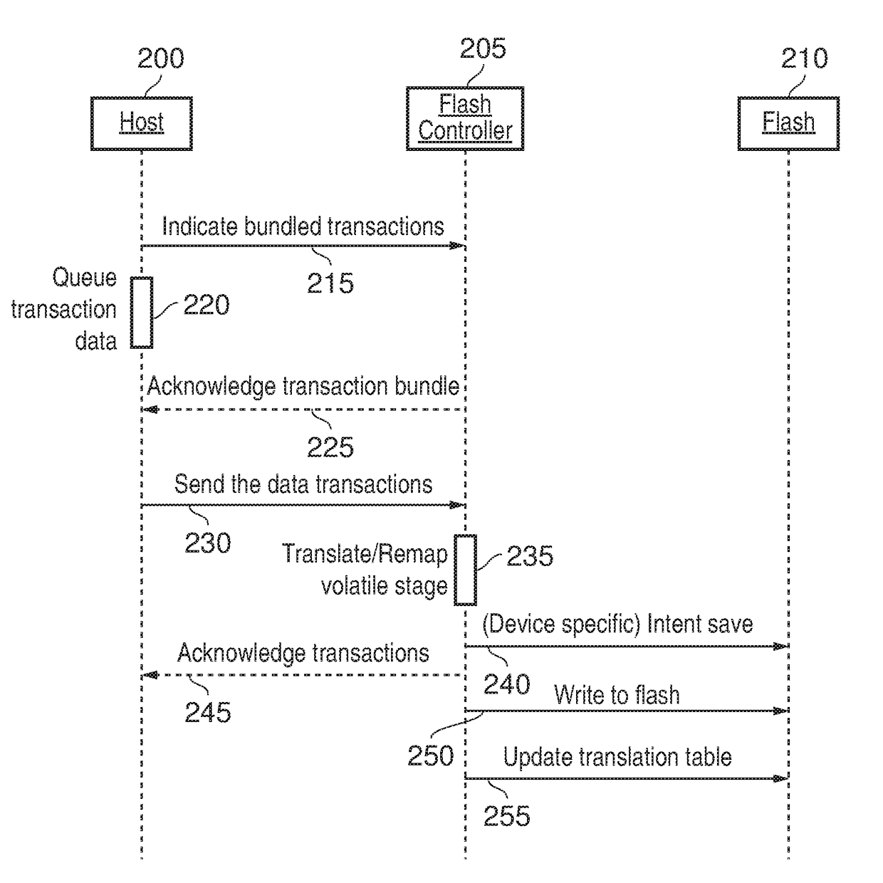
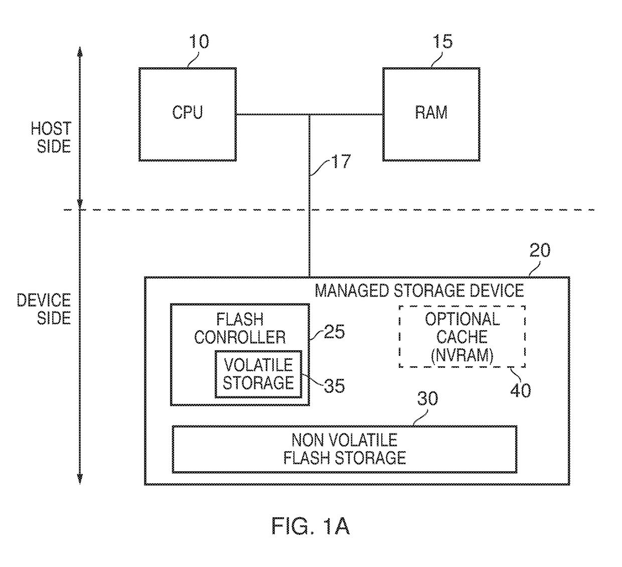
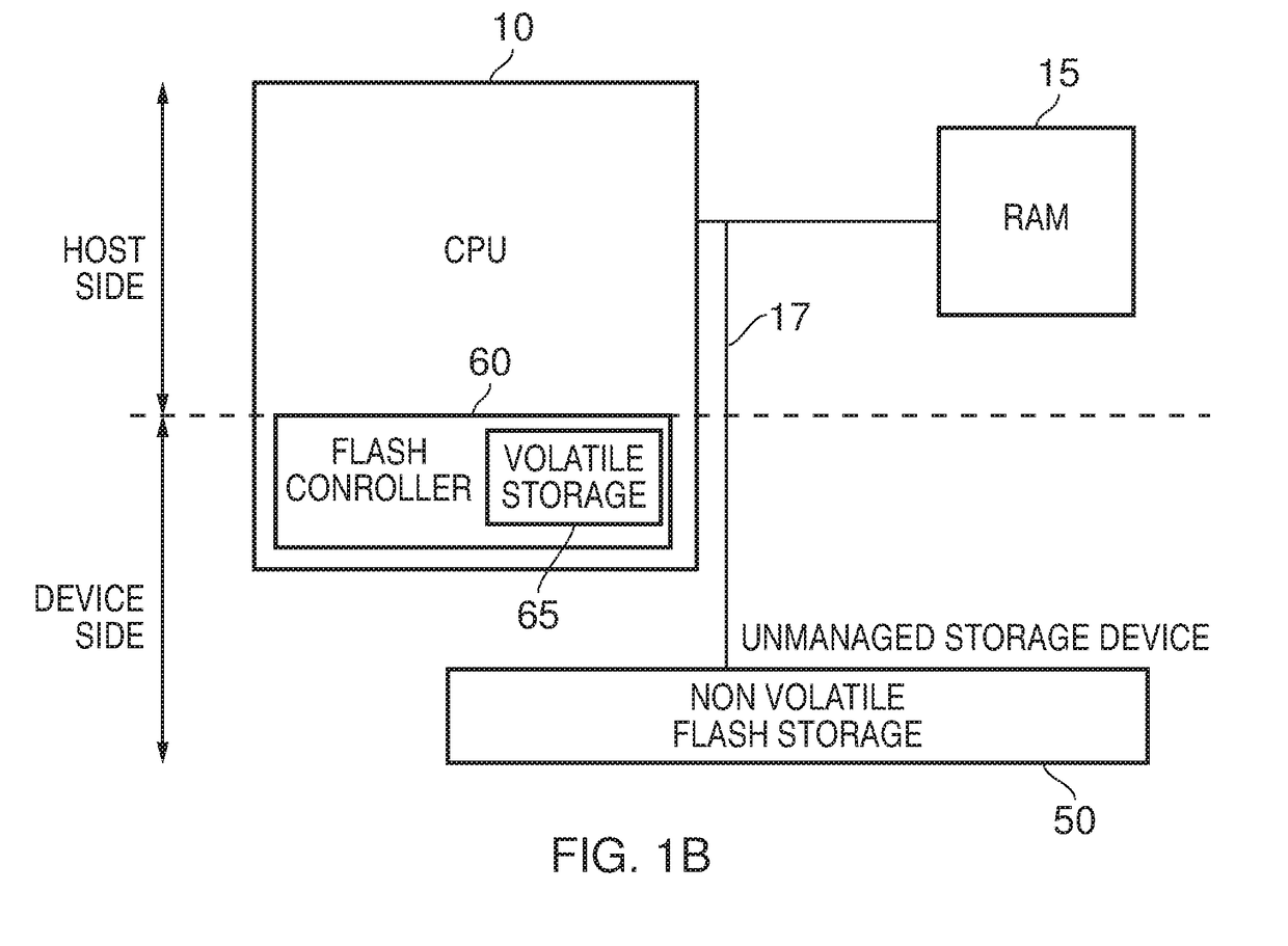
[0048]FIG. 1A is a block diagram of a system in accordance with one embodiment. In this embodiment, it is assumed that the non-volatile data storage device 20 takes the form of a managed storage device with its own internal device controller 25 for controlling the performance of write transactions to the non-volatile storage 30. In this particular example, it is assumed that the non-volatile storage 30 is non-volatile flash storage, and accordingly the device controller 25 is a flash controller. Flash memory is typically formed from NAND devices, and is arranged as a plurality of blocks, such as the blocks 72, 73, 74, 75, 76 shown for example in FIG. 1C for the flash storage 70. Within each block there are a plurality of pages 82, 84, 86.

[0049]NAND flash memory is page readable and programmable. Read actions typically take about ten times less than write actions. Further, once a page has been written to, it has to be erased before new data can be written to that page again, and acco...


PUM


Abstract

A device controller and method are provided for performing a plurality of write transactions atomically within a non-volatile data storage device. Each transaction specifies a logical address and the method comprises creating an address translation map for the logical addresses specified by the plurality of write transactions, by referencing an address translation record within the non-volatile data storage device to determine for each logical address a corresponding physical address within the data storage device. Further, if the corresponding physical address indicated in the address translation record already contains valid data, the logical address is remapped to a new physical address in the address translation map. However, at this point the address translation record as stored in the data storage device is not updated. Instead, the plurality of write transactions are performed using the logical address to physical address mapping in the address translation map. Then, only once the plurality of write transactions have been performed is the address translation record updated in the non-volatile data storage device in order to identify the logical address to physical address mapping in the address translation map. Since, at the time of performing the write transactions, any new data that updates data already stored in the data storage device is written into a different physical address location, and hence the previous version of the data is still stored on the data storage device, and given that the address translation record is not updated unless the plurality of write transactions are actually performed atomically, then this enables the state held on the data storage device to be rolled back to the state that existed prior to performing the plurality of write transactions, if any event prevents that plurality of write transactions being performed atomically.

Description

FIELD OF THE INVENTION[0001]The present invention relates to a device controller and method for performing a plurality of write transactions atomically within a non-volatile data storage device.BACKGROUND OF THE INVENTION[0002]There are a number of situations where it is desirable to perform multiple write transactions to different locations within a non-volatile data storage device atomically. For example, this may be due to the data files being written being too large to fit in one location, or due to an operation requiring updates in multiple locations. An example of this latter scenario is when a new file is created in a folder. The file needs to be written to the appropriate location in the non-volatile storage device, but in addition the metadata describing the folder structure in which the file is located also needs to be updated. Completion of one of these steps without the other (for instance due to a system crash) would either result in the file system indicating that ther...

Claims


Application Information

Patent Timeline
IPC IPC(8): G06F3/06G06F12/10G06F12/02G06F12/0802
CPCG06F3/061G06F3/0656G06F3/0679G06F12/0802G06F2212/65G06F12/0253G06F12/0246G06F2212/222G06F12/10G06F12/1009G06F12/1045G06F12/1054G06F12/1063G06F13/16G06F2212/7201G06F3/0619G06F3/064G06F12/0238G11C16/06G06F3/06G06F9/467
Inventor DE JONG, IRENEUS JOHANNESHANSSON, ANDREAS
Owner ARM LTD
Why Eureka
Try Eureka