Contacting Apparatus for Contacting An Energy Storage Cell
- Summary
- Abstract
- Description
- Claims
- Application Information
AI Technical Summary
Benefits of technology
Problems solved by technology
Method used
Image
Examples
fifth embodiment
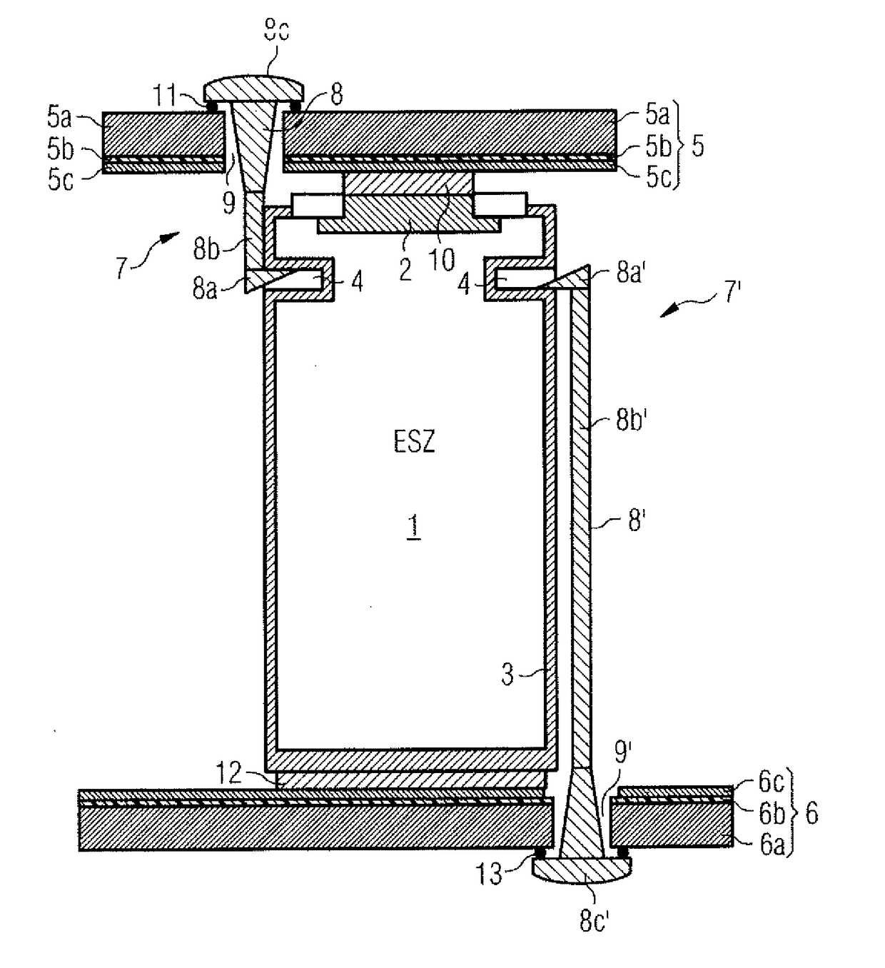
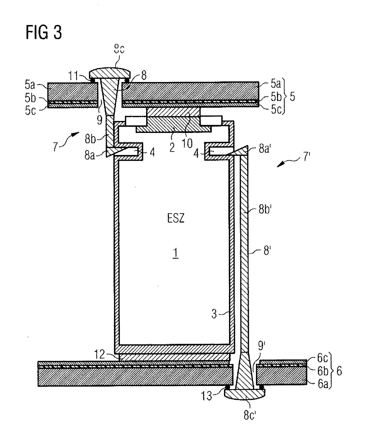
[0056]FIG. 8 shows a fifth embodiment variant of the contacting apparatus in accordance with the invention comprising an SMD (Service Mounted Device)-clip 8 having a clip hook 8a which engages into the circumferential groove 4 of the energy storage cell 1. In the case of this embodiment variant, the SMD-clip 8 engages with its clip hook 8a into the outer groove 4 of the energy storage cell 1 and thus produces a defined contact pressing force F. In the case of the embodiment variant illustrated in FIG. 8, the clip 8 is attached, e.g. soldered, to the electrically conductive layer 5c which consists e.g. of copper. THE SMD-clip 8 can consist e.g. of a non-metallic material which is provided on a metallic carrier of the SMD-clip 8 which, for its part, is soldered to the electrically conductive layer 5c of the printed circuit board 5. In the case of the embodiment variant illustrated in FIG. 8, the negative pole 3 can be contacted via a second printed circuit board (not illustrated).
sixth embodiment
[0057]FIG. 9 shows a further sixth embodiment variant of the contacting apparatus in accordance with the invention, in which the SMD-clips 8 of the releasable mechanical clip connection 7 engage at the positive pole 2 of the energy storage cell 1. In the case of this embodiment variant, the positive pole2 of the energy storage cell 1 has holes which are produced during manufacture and into which a clip hook 8a of an SMD-clip 8 can latch in each case. A required contact pressing force F can be produced in this manner. In the case of the embodiment variant illustrated in FIG. 9, the SMD-clip 8 consists of a metallic, electrically conductive material. The metallic SMD-clip 8 is soldered or fixedly soldered to the copper layer 5c of the printed circuit board 5. In the case of the embodiment variant illustrated in FIG. 9, the negative pole 3 of the energy storage cell 1 is preferably contacted by means of a further printed circuit board, not illustrated.
seventh embodiment
[0058]FIG. 10 shows a further seventh embodiment variant of the contacting apparatus in accordance with the invention. In the case of this embodiment variant, the SMD-clips 8 engage into an outer groove 4 of the energy storage cell 1. Both the positive pole 2 and the negative pole 3 are contacted by means of the SMD-clips 8 with a single printed circuit board 5. In the case of the embodiment variant illustrated in FIG. 10, the releasable mechanical connection 7 thus has at least two SMD-clips 8, 8′ which each comprise an electrically conductive component and contact the positive pole 2 and the negative pole 3 of the energy storage cell 1. The releasable mechanical connection 7 has an inner clip 8′ for the positive pole 2 and an outer clip 8 for the negative pole 3 of the energy storage cell 1. An electrically insulating layer or an electrically insulating component 19b is provided between the two electrically conductive components which form the two SMD-clips 8, 8′. In the case of t...
PUM
 Abstract
Description
Claims
Application Information


