Supercharge Your Innovation With Domain-Expert AI Agents!

Goa circuit based on oxide semiconductor thin film transistor

Active Publication Date: 2017-07-27
SHENZHEN CHINA STAR OPTOELECTRONICS TECH CO LTD
View PDF6 Cites 7 Cited by
  • Summary
  • Abstract
  • Description
  • Claims
  • Application Information

AI Technical Summary

Benefits of technology

The present invention provides a new GOA circuit that uses oxide semiconductor thin film transistors. By adding certain transistors, the circuit can prevent the pull-down holding module from being unable to be deactivated because of a forward-biased threshold voltage. This ensures that the circuit can output normal results.

Problems solved by technology

Thus, the design difficulty of the GOA circuit based on the oxide semiconductor thin film transistor will be increased.
There will be some function issues happening when the design adaptable to the scan driving circuit for the amorphous silicon semiconductors is applied to the GOA circuit based on the oxide semiconductor thin film transistor.
Besides, due to some external factor inductions and the stress effect, there will be a tendency that the threshold voltage diminishes toward minus value to the oxide semiconductor thin film transistor, which may directly result in malfunction of the GOA circuit for the oxide semiconductor thin film transistors.
However, the GOA circuit based on oxide semiconductor thin film transistor remains a certain problem existing: the pull-down holding module 600 utilizes the signal of the first node Q(N) to control the ability of pull-down and deactivation.
Accordingly, the first node Q(N) cannot be normally boosted up to the high voltage level in the functioning period, which results in the bad performance of the entire GOA circuit.

Method used


Image

  • Goa circuit based on oxide semiconductor thin film transistor
  • Goa circuit based on oxide semiconductor thin film transistor
  • Goa circuit based on oxide semiconductor thin film transistor

Examples


Embodiment Construction

[0053]For better explaining the technical solution and the effect of the present invention, the present invention will be further described in detail with the accompanying drawings and the specific embodiments.

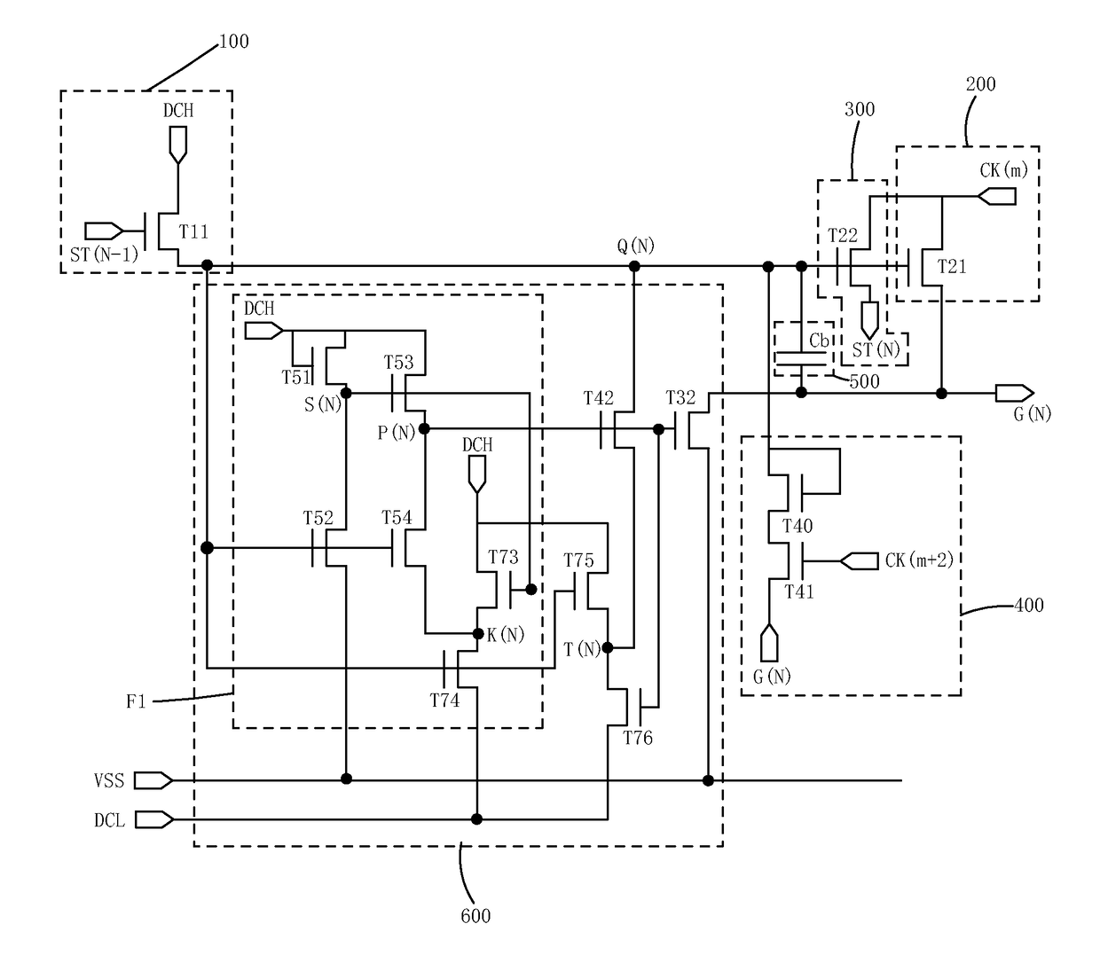
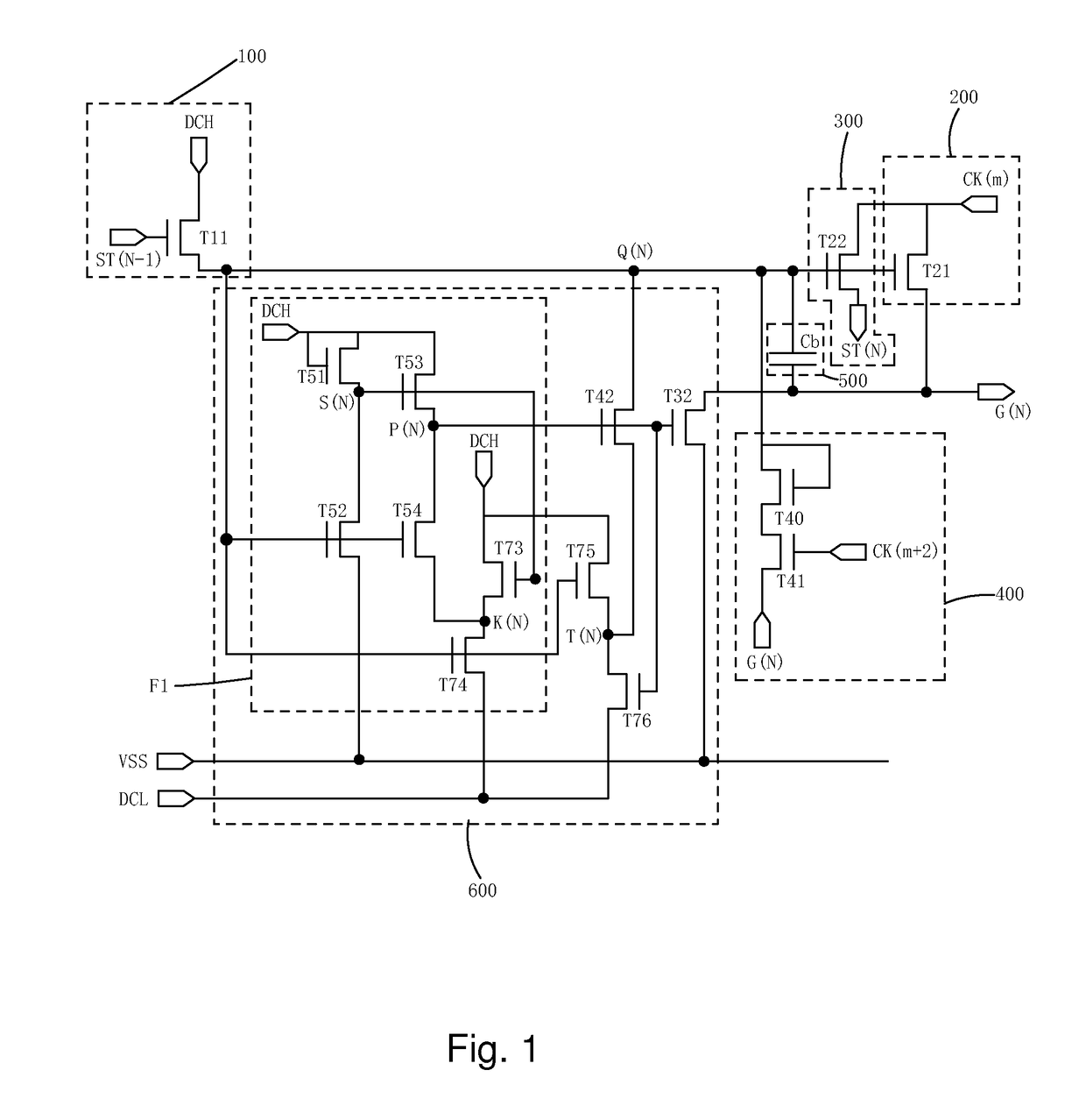
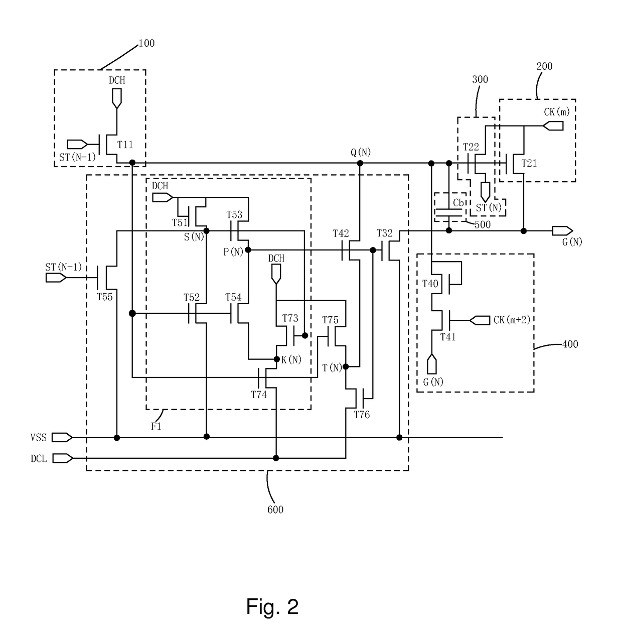
[0054]The present invention provides a GOA circuit based on oxide semiconductor thin film transistor. Please refer to FIG. 2. FIG. 2 is a circuit diagram of the first embodiment according to a GOA circuit based on oxide semiconductor thin film transistor of the present invention, comprising a plurality of GOA unit circuits which are cascade connected, and the GOA unit circuit of every stage comprises a pull-up controlling module 100, a pull-up module 200, a transmission module 300, a first pull-down module 400, a bootstrap capacitor module 500 and a pull-down holding module 600.

[0055]N is set to be a positive integer and except the GOA unit circuit of the first stage, in the GOA unit circuit of the Nth stage:

[0056]the pull-up controlling module 100 comprises: an eleventh thin ...


PUM


Abstract

The present invention provides a GOA circuit based on oxide semiconductor thin film transistor. By adding the fifty-fifth, fifty-sixth, fifty-seventh thin film transistors (T55, T56, T57) respectively corresponding to the fourth, fifth, second nodes (S(N), K(N), P(N)) in the pull-down holding module (600). The fifty-fifth, fifty-sixth, fifty-seventh thin film transistors (T55, T56, T57) are controlled with the stage transfer signal of the GOA unit circuit of the former N−1th stage or the scan driving signal of the GOA unit circuit of the former N−1th stage to pull down the voltage levels of the fourth, fifth, second nodes (S(N), K(N), P(N)) under circumstance that the first node (Q(N)) is not completely boosted to rapidly deactivate the pull-down holding module (600) for ensuring the normal boost of the voltage level of the first node (Q(N)). The first node (Q(N)) is guaranteed to be high voltage level in the functioning period, and thus, the normal output of the GOA circuit is ensured.

Description

FIELD OF THE INVENTION[0001]The present invention relates to a display technology field, and more particularly to a GOA circuit based on oxide semiconductor thin film transistor.BACKGROUND OF THE INVENTION[0002]The Liquid Crystal Display (LCD) possesses advantages of thin body, power saving and no radiation to be widely used in many application scope, such as LCD TV, mobile phone, personal digital assistant (PDA), digital camera, notebook, laptop, and dominates the flat panel display field.[0003]The Active Matrix Liquid Crystal Display (AMLCD) is the most common liquid crystal display device at present. The Active Matrix Liquid Crystal Display comprises a plurality of pixels, and each pixel is electrically coupled to a Thin Film Transistor (TFT). The gate (Gate) of the TFT is coupled to the horizontal scan line. The drain (Drain) of the TFT is coupled to the data line of the vertical direction. The source (Source) of the TFT is coupled to the pixel electrode. The enough voltage is a...

Claims


Application Information

Patent Timeline
IPC IPC(8): G09G3/36
CPCG09G3/3677G09G2300/043G09G2300/0809G09G2300/0408G09G3/36G09G2310/08G09G2310/0286G09G2310/0289G09G2310/0264G09G2310/02
Inventor DAI, CHAO
Owner SHENZHEN CHINA STAR OPTOELECTRONICS TECH CO LTD
Features
  • R&D
  • Intellectual Property
  • Life Sciences
  • Materials
  • Tech Scout
  • Unparalleled Data Quality
  • Higher Quality Content
  • 60% Fewer Hallucinations
Learn More