

Multiplexed pixel column architecture for imagers
a multi-pixel column and imager technology, applied in the field of imaging devices, can solve the problems of increasing the frequency of the switching in the readout path, increasing the readout noise of imagers, and more power consumption than desired, so as to reduce the noise and power consumption of readouts, simplify the column select circuitry, and speed up the readout speed
- Summary
- Abstract
- Description
- Claims
- Application Information
AI Technical Summary
Benefits of technology
Problems solved by technology
Method used
Image

Examples
Embodiment Construction
[0037] In the following detailed description, reference is made to the accompanying drawings, which are a part of the specification, and in which is shown by way of illustration various embodiments whereby the invention may be practiced. These embodiments are described in sufficient detail to enable those skilled in the art to make and use the invention. It is to be understood that other embodiments may be utilized, and that structural, logical, and electrical changes, as well as changes in the materials used, may be made without departing from the spirit and scope of the present invention.
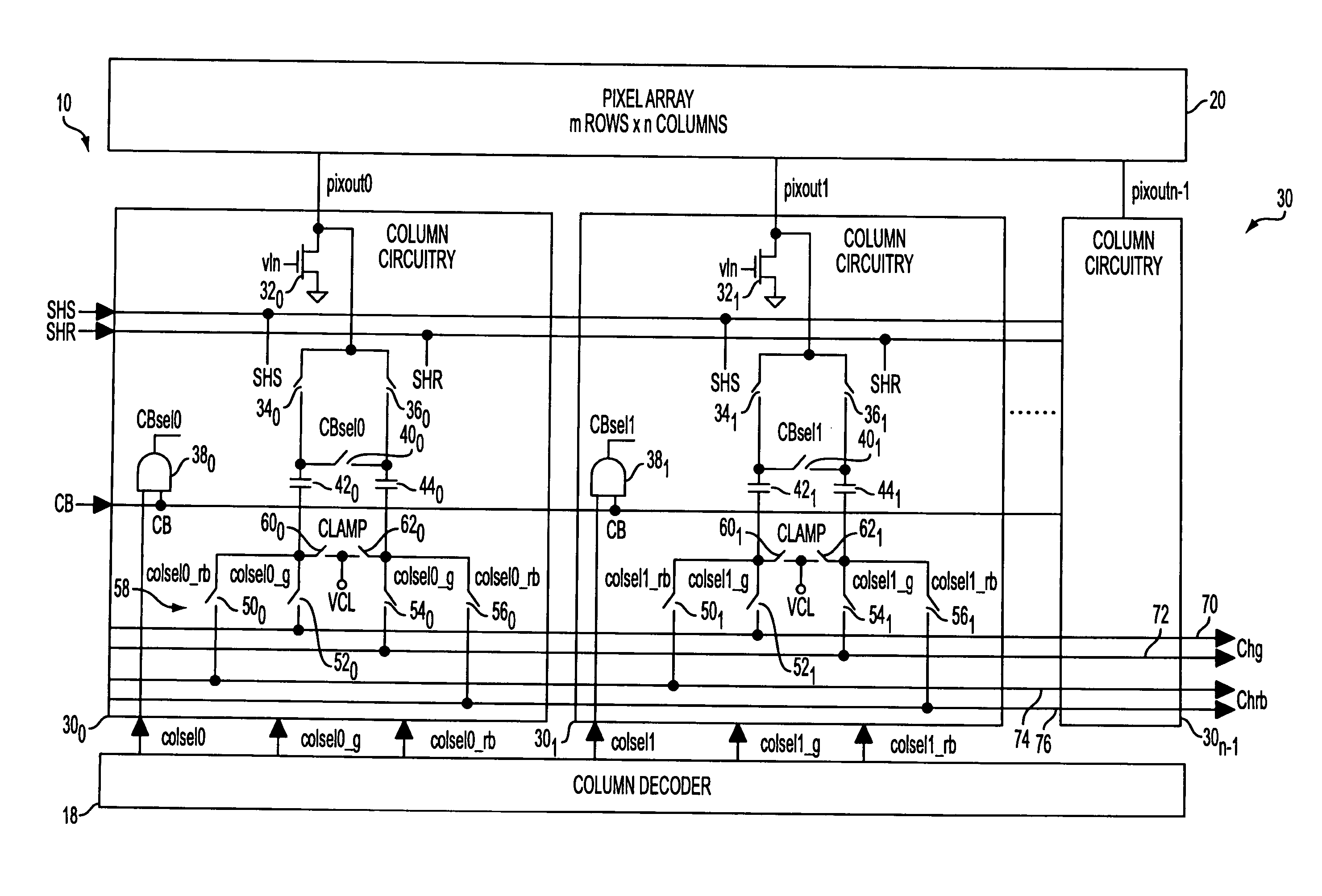
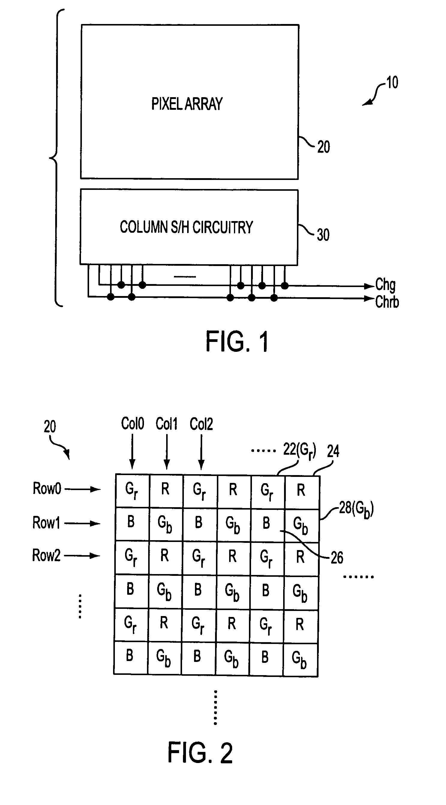
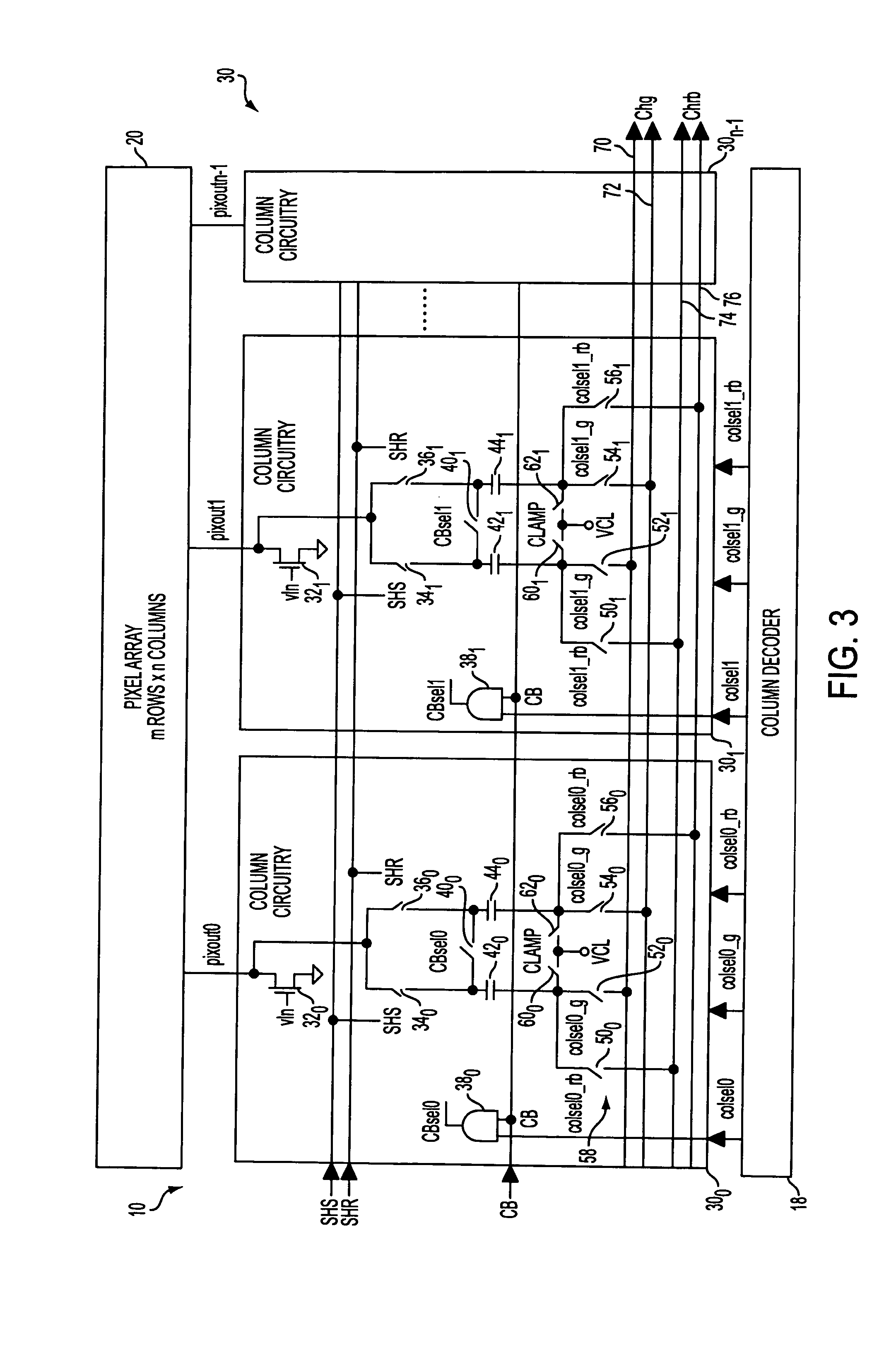
[0038] Now referring to the figures, where like reference numbers designate like elements, FIG. 4 shows a CMOS imager 110 constructed in accordance with a first exemplary embodiment of the invention. The imager 110 includes a pixel array 20, column decoder 118, column S / H circuitry 130 and a multiplexer 180. The imager 110 has two output channels Chg, Chrb. The first channel Chg includes two outp...
PUM
 Abstract
Description
Claims
Application Information