Graphene-based laminate and method of preparing the same
- Summary
- Abstract
- Description
- Claims
- Application Information
AI Technical Summary
Benefits of technology
Problems solved by technology
Method used
Image
Examples
example 3
on of Graphene-Based Laminate
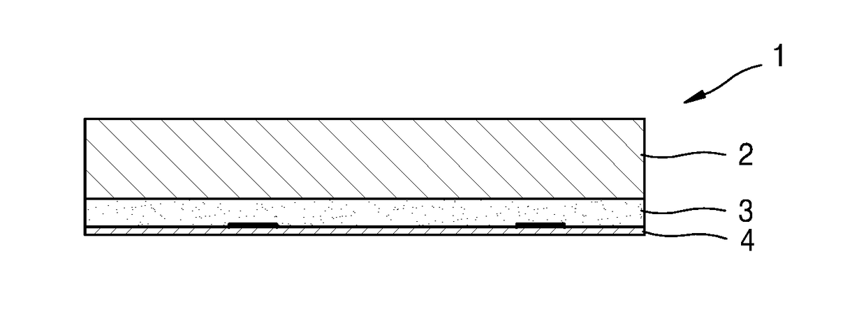
[0123]A graphene-based laminate was prepared in the same manner as in Example 1, except that a thickness of the LiF layer deposited on the graphene layer was 10 nm instead of 1 nm.
example 4
on of Back-Gated FET
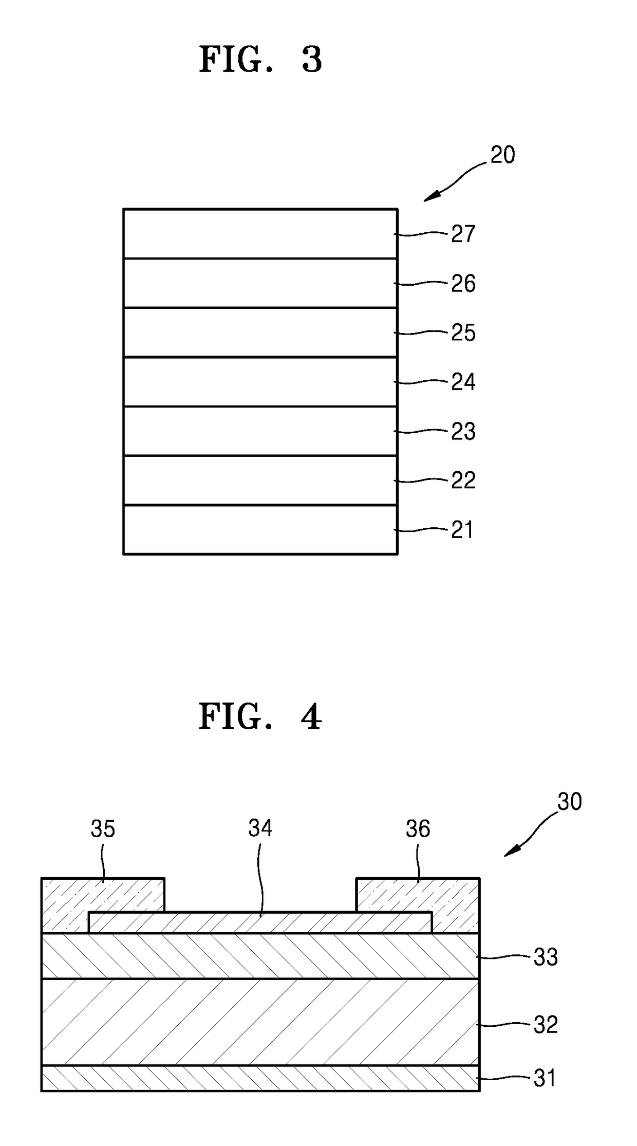
[0126]The back-gated FET shown in FIG. 4 was prepared.
[0127]100 nm of Au patterned by a lift-off process using a photoresist AZ5214 was used as a source electrode and a drain electrode. As a channel layer, the graphene-based laminate prepared in Example 1 was used. A length and width of the channel layer was 20 μm and 19 μm, respectively. The insulating layer was SiO2 having a thickness of 300 nm.
examples 5 and 6
ack-Gated FET
[0128]Back-gated FETs were prepared in the same manner as in Example 4, except that the graphene-based laminates prepared in Examples 2 and 3 were respectively used as a channel layer instead of the graphene-based laminate prepared in Example 1.
PUM
 Abstract
Description
Claims
Application Information


