Access Resistance Modulated Solid-State Light Source

a solid-state light source and access resistance technology, applied in the field of solid-state light sources, can solve the problems of limiting the modulation time, optical pulse distortion, external driver circuit weight and cost to the ssls system,

Active Publication Date: 2017-08-31
SENSOR ELECTRONICS TECH
View PDF3 Cites 3 Cited by
  • Summary
  • Abstract
  • Description
  • Claims
  • Application Information

AI Technical Summary

Benefits of technology

[0006]Aspects of the invention provide a solid-state light source with built-in access resistance modulation. The light source can include an active region configured to emit electromagnetic radiation during operation of the light source. The active region can be formed at a p-n junction of a p-type side with a p-type contact and a n-type side with a n-type contact. The light source includes a control electrode configured to modulate an access resistance of an access region located on the p-type side and/or an access resistance of an access region located on the n-type side of the active region. The solid-state light source can be implemented in a circuit, which includes a voltage source that supplies a modulation voltage to the control electrode to modulate the access resistance(s).
[0007]A first aspect of the invention provides a solid-state light source comprising: an active region configured to emit electromagnetic radiation during operation of the light source; a n-type contact located on a n-type side of the active region and separated from the active region by a n-type access region; a p-type contact located on a p-type side of the active region and separated from the active region by a p-type access region; and a control electrode configured to modulate at least one of: an access resistance of the n-type access region or an access resistance of the p-type access region.
[0008]A second aspect of the invention provides a circuit comprising: a solid-state light source comprising: an active region configured to emit electromagnetic radiation during operat...

Problems solved by technology

However, using external driver circuits results in parasitic parameters, which limit the modulation time and cause ringing and optical pulse distortions.
Additionally, the external driver circuits as weight a...

Method used


Image

  • Access Resistance Modulated Solid-State Light Source
  • Access Resistance Modulated Solid-State Light Source
  • Access Resistance Modulated Solid-State Light Source

Examples


Embodiment Construction

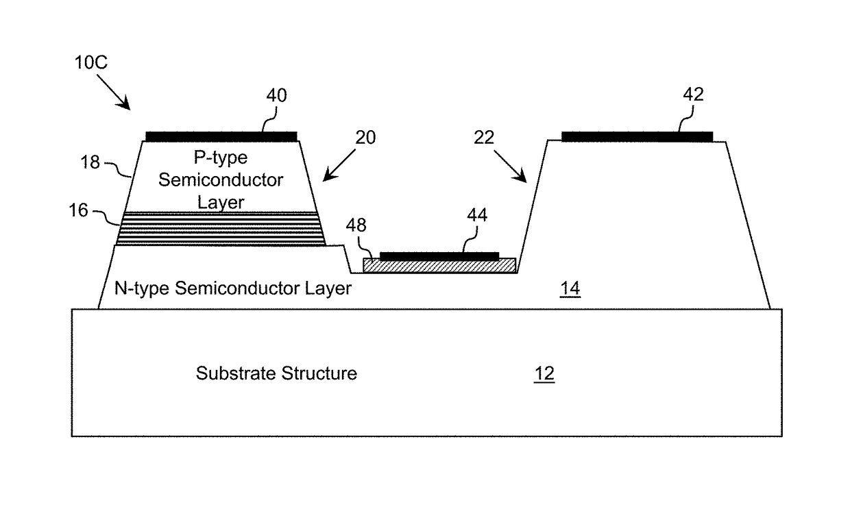
[0027]As indicated above, aspects of the invention provide a solid-state light source with built-in access resistance modulation. The light source can include an active region configured to emit electromagnetic radiation during operation of the light source. The active region can be formed at a p-n junction of a p-type side with a p-type contact and a n-type side with a n-type contact. The light source includes a control electrode configured to modulate an access resistance of an access region located on the p-type side and / or an access resistance of an access region located on the n-type side of the active region. The solid-state light source can be implemented in a circuit, which includes a voltage source that supplies a modulation voltage to the control electrode to modulate the access resistance(s).

[0028]As used herein, unless otherwise noted, the term “set” means one or more (i.e., at least one) and the phrase “any solution” means any now known or later developed solution. It i...


PUM


Abstract

A solid-state light source with built-in access resistance modulation is described. The light source can include an active region configured to emit electromagnetic radiation during operation of the light source. The active region can be formed at a p-n junction of a p-type side with a p-type contact and a n-type side with a n-type contact. The light source includes a control electrode configured to modulate an access resistance of an access region located on the p-type side and/or an access resistance of an access region located on the n-type side of the active region. The solid-state light source can be implemented in a circuit, which includes a voltage source that supplies a modulation voltage to the control electrode to modulate the access resistance(s).

Description

REFERENCE TO RELATED APPLICATIONS[0001]The current application claims the benefit of U.S. Provisional Application No. 62 / 301,041, which was filed on 29 Feb. 2016, and which is hereby incorporated by reference.TECHNICAL FIELD[0002]The disclosure relates generally to solid-state light sources, and more particularly, to a solid-state light source with access resistance modulation.BACKGROUND ART[0003]A great deal of interest has been focused on solid-state light sources (SSLSs), such as LEDs and lasers, and in particular, those that emit light in the blue and deep ultraviolet (UV) wavelengths. These devices may be capable of being incorporated into various applications, including solid-state lighting, biochemical disinfection and detection, high-density data storage, and the like.[0004]Modern SSLSs, such as an LEDs, typically include three major components: an electron supply layer (e.g., a n-type semiconductor layer), a hole supply layer (e.g., a p-type semiconductor layer), and a ligh...

Claims


Application Information

Patent Timeline
IPC IPC(8): H05B33/08H01L33/14H01S5/30H01L33/32H01L33/06H01S5/042H01L33/38H01L33/24H05B44/00
CPCH05B33/0842H01L33/382H01L33/14H01L33/24H01S5/3013H01L33/06H01S5/0425H01S5/0427H01L33/32H01L33/38H01L33/20H05B45/325H01S5/06203H01L33/36H01S5/0614
Inventor SHUR, MICHAELSIMIN, GRIGORY
Owner SENSOR ELECTRONICS TECH
Why Eureka
Try Eureka