Semiconductor device and manufacturing method therefor

Active Publication Date: 2017-09-07
DENSO CORP
View PDF6 Cites 1 Cited by
  • Summary
  • Abstract
  • Description
  • Claims
  • Application Information

AI Technical Summary

Benefits of technology

[0014]According to the manufacturing method of the semiconductor device configured as above, the first wiring layer and the thin-film resistor are provided, respectively, in the step of providing the first wiring layer and the step of providing the lower oxidation preventing film, the thin-film resistor, and the upper oxidation preventing film in such a manner that the first wiring layer has a portion overlapping the end portions of the thin-film resistor when viewed in a direction normal to the one surface of the substrate. Hence, in comparison with a case where the first wiring layer is not provided in the portion specified a

Problems solved by technology

Consequently, oxidation on the side surfaces of the thin-film resistor can be restricted, which can in turn restrict a variance in resistance value of the thin-f

Method used


Image

  • Semiconductor device and manufacturing method therefor
  • Semiconductor device and manufacturing method therefor
  • Semiconductor device and manufacturing method therefor

Examples


first embodiment

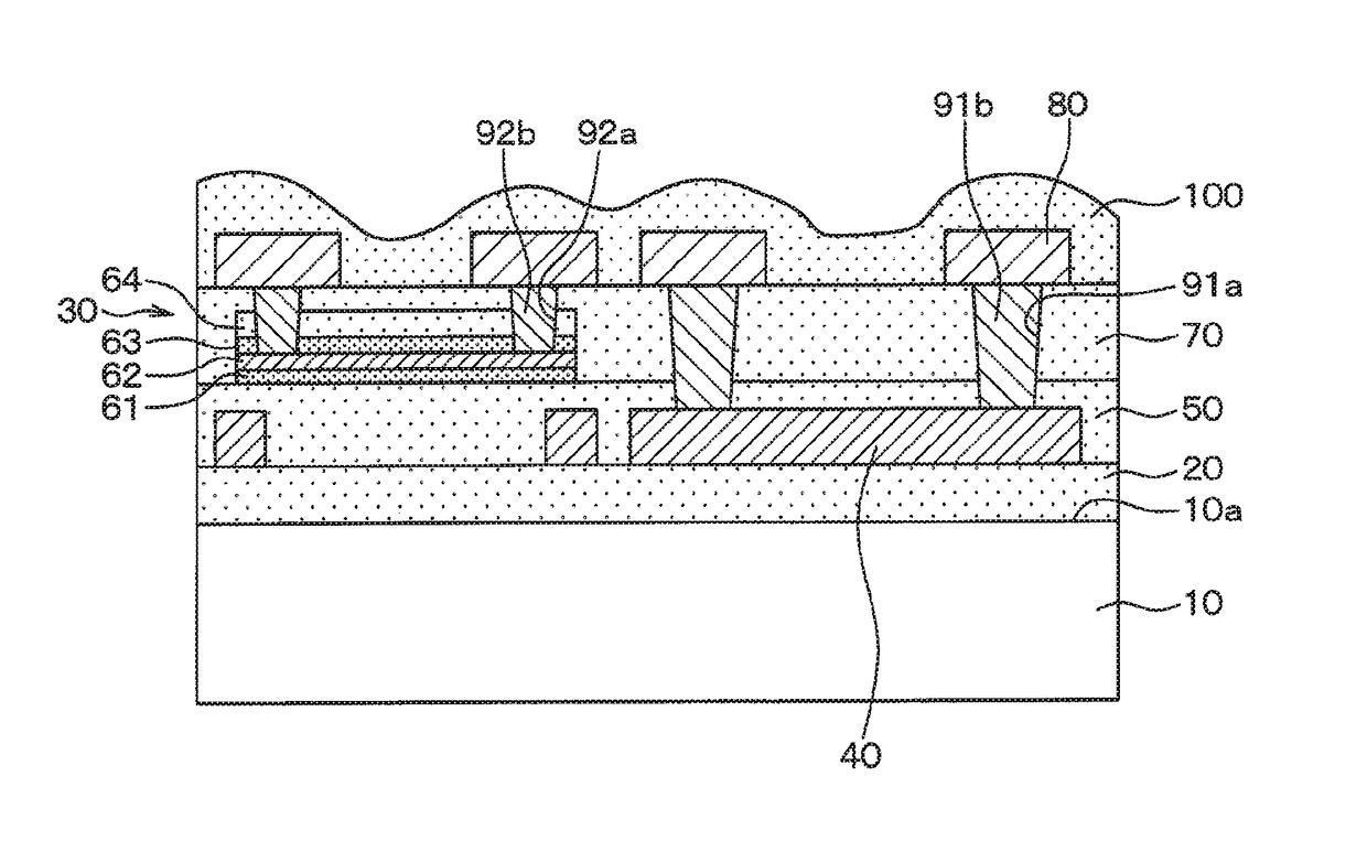
[0033]A first embodiment of the present disclosure will be described with reference to the drawings. As is shown in FIG. 1, a semiconductor device has a substrate 10 formed of a silicon substrate or the like and the substrate 10 is provided with unillustrated semiconductor elements, such as diodes and transistors. A multi-layer wiring layer 30 having a thin-film resistor 62 inside is disposed on one surface 10a of the substrate 10 via an oxide film 20.

[0034]More specifically, a first wiring layer 40 made of Al, Al—Cu alloy, Cu, W, Ti, Au, Pt, or the like is appropriately patterned and disposed on the oxide film 20. A first insulating film 50 made of TEOS or the like is disposed so as to cover the first wiring layer 40.

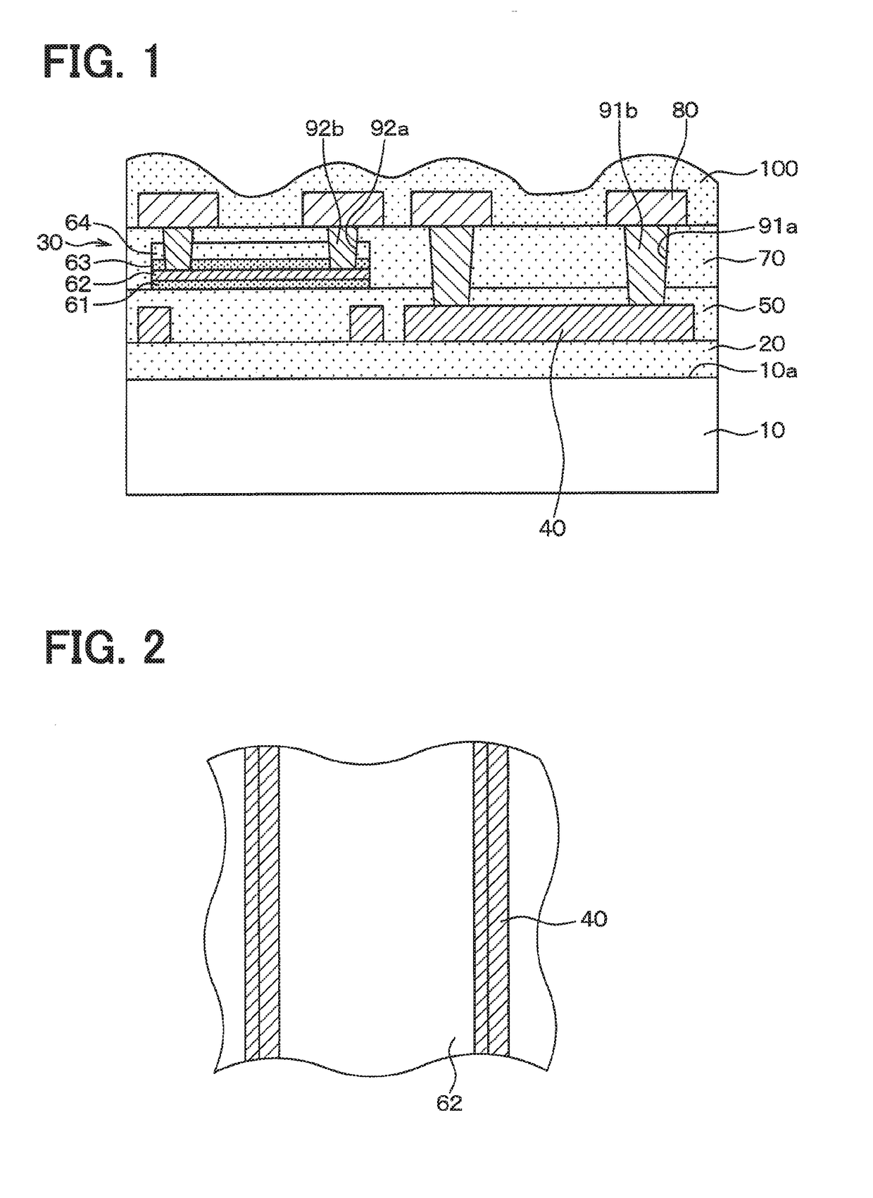
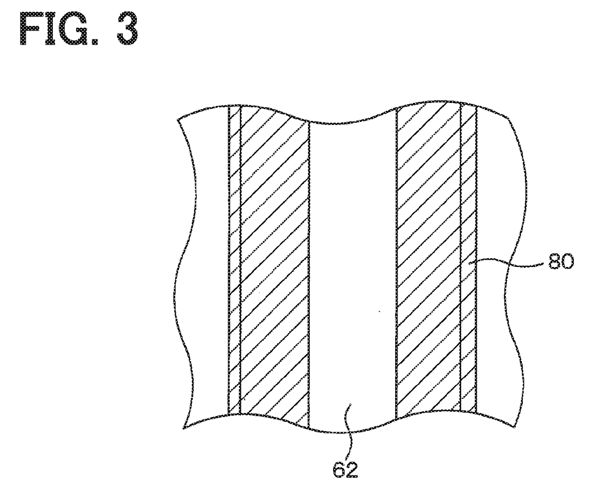
[0035]In a predetermined region on the first insulating film 50, a lower oxidation preventing film 61, the thin-film resistor 62, an upper oxidation preventing film 63, and a second insulating film 64 are sequentially laminated. In short, the thin-film resistor 62 is d...

second embodiment

[0070]A second embodiment of the present disclosure will be described. The present embodiment is different from the first embodiment above in that multiple thin-film resistors 62 are provided and paired resistance is formed using the multiple thin-film resistors 62. A rest of the present embodiment is same as the first embodiment above and a description is not repeated herein.

[0071]FIG. 11 is a top view of a semiconductor device of the present embodiment and shows a positional relation of first and second wiring layers 40 and 80 and thin-film resistors 111 through 118. FIG. 11 is not a sectional view. However, the first and second wiring layers 40 and 80 are shaded and a protection film 100 is omitted for ease of understanding.

[0072]In the present embodiment, as is shown in FIG. 11, the first through eighth thin-film resistors 111 through 118 are provided sequentially along a first direction (right-left direction on a sheet surface of FIG. 11) in a plane direction of a substrate 10....


PUM


Abstract

A semiconductor device includes: a substrate; a first wiring layer arranged above the substrate; a first insulating film covering the first wiring layer; a lower oxidation preventing film arranged on the first insulating film; at least one thin-film resistor arranged on the lower oxidation preventing film; an upper oxidation preventing film arranged on the at least one thin-film resistor; a second insulating film covering the lower oxidation preventing film, the at least one thin-film resistor, and the upper oxidation preventing film; a second wiring layer arranged on the second insulating film; and a third insulating film covering the second wiring layer. The first wiring layer overlaps an end portion of the at least one thin-film resistor when viewed in a normal direction of one surface of the substrate.

Description

CROSS REFERENCE TO RELATED APPLICATIONS[0001]This application is a U.S. national stage application of International Patent Application No. PCT / JP2015 / 005036 filed on Oct. 2, 2015 and is based on Japanese Patent Application No. 2014-206425 filed on Oct. 7, 2014, and No. 2015-176741 filed on Sep. 8, 2015, the disclosures of which are incorporated herein by reference.TECHNICAL FIELD[0002]The present disclosure relates to a semiconductor device having a thin-film resistor on one surface of a substrate and a manufacturing method of such a semiconductor device.BACKGROUND ART[0003]A semiconductor device in the related art includes a multi-layer wiring layer formed by laminating wiring layers made of Al or the like, insulating films made of TEOS (Tetra Ethyl Ortho Silicate) or the like, and so on on one surface of a substrate. A thin-film resistor made of CrSi or the like is provided inside the multi-layer wiring layer along a plane direction of the substrate. In the semiconductor device as...

Claims


Application Information

Patent Timeline
IPC IPC(8): H01L23/00H01L23/522H01L49/02
CPCH01L23/564H01L23/5228H01L28/24H01C7/006H01L27/016H01L27/0802H01L27/101H01L28/20
Inventor TAKIZAWA, SHINNAKANO, TAKASHI
Owner DENSO CORP
Why Eureka
Try Eureka