Electronic device including graphene-based layer(s), and/or method or making the same

a graphene-based layer, electronic device technology, applied in the direction of sustainable manufacturing/processing, instruments, final product manufacturing, etc., can solve the problems of inability to use ito and fto, and inability to meet the requirements of the near infrared region

Inactive Publication Date: 2011-02-10
GUARDIAN GLASS LLC
View PDF101 Cites 78 Cited by
  • Summary
  • Abstract
  • Description
  • Claims
  • Application Information

AI Technical Summary

Benefits of technology

[0003]Thus, it will be appreciated that there is a need in the art for smooth and patternable electrode materials with good stability, high transparency, and excellent conductivity.
[0020]In certain example embodiments, the graphene-based layer is transferred to a second substrate prior to the patterning. In certain example embodiments, the patterning is performed to reduce conductivity and / or remove portions of the graphene-based layer.

Problems solved by technology

Unfortunately, however, the use of ITO and FTO is becoming increasingly problematic for a number of reasons.
Such problems include, for example, the fact that there is a limited amount of the element indium available on Earth, the instability of the TCOs in the presence of an acide or base, their susceptibility to ion diffusion from ion conducting layers, their limited transparency in the near infrared region (e.g., power-rich spectrum), high leakage current of FTO devices caused by FTO structure defects, etc.
The brittle nature of ITO and its high deposition temperature can also limit its applications.
In addition, surface asperities in SnO2:F may cause problematic arcing.
However, there are drawbacks with the exfoliation process.
For example, exfoliated graphene tends to fold and become crumpled, exists as small strips and relies on a collage / stitch process for deposition, lacks inherent control on the number of graphene layers, etc.
The material so produced is often contaminated by intercalates and, as such, has low grade electronic properties.

Method used


Image

  • Electronic device including graphene-based layer(s), and/or method or making the same
  • Electronic device including graphene-based layer(s), and/or method or making the same
  • Electronic device including graphene-based layer(s), and/or method or making the same

Examples


example process

Flow

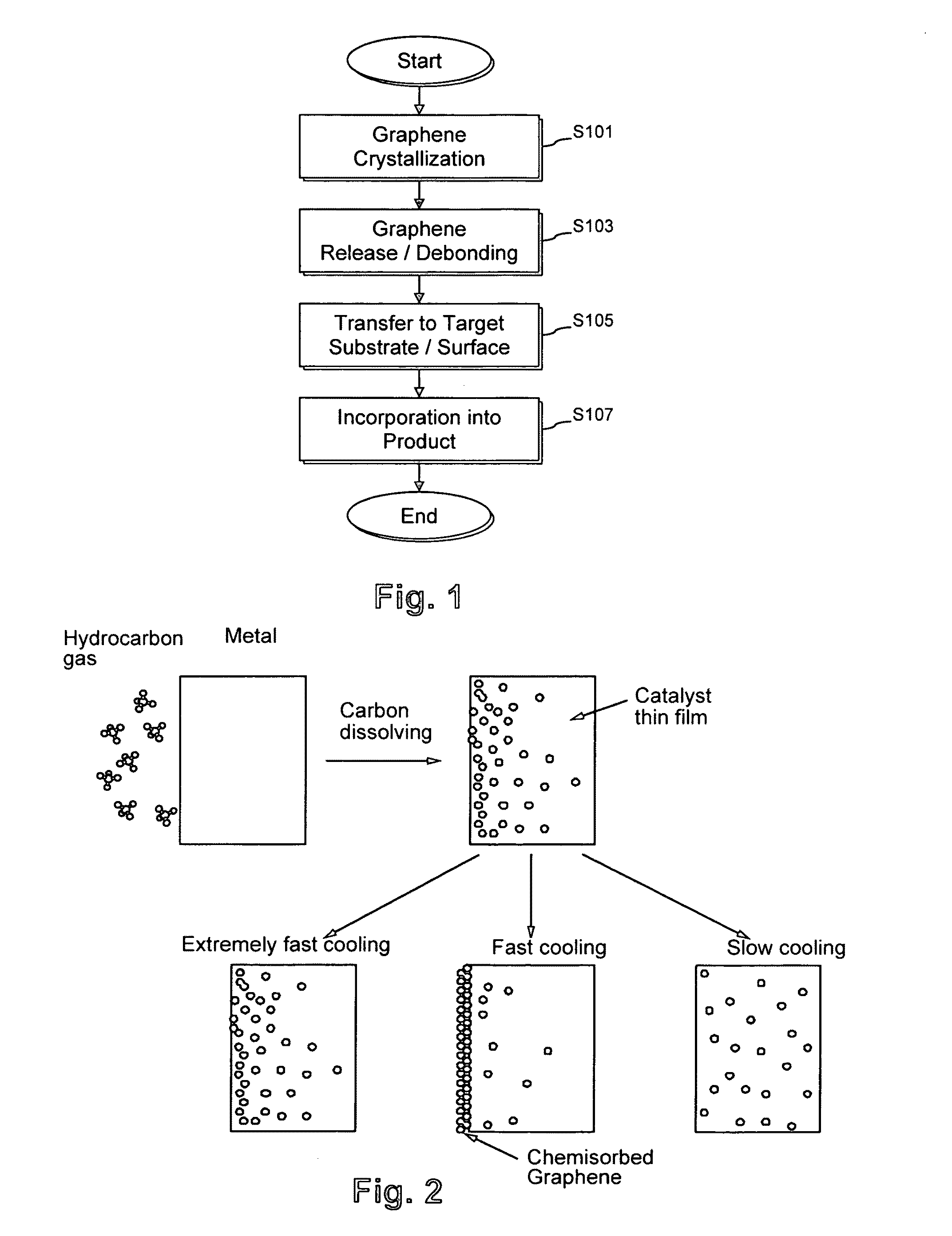
[0072]FIG. 10 is an example process flow that illustrates certain of the example catalytic CVD growth, lift-off, and transfer techniques of certain example embodiments. The example process shown in FIG. 10 begins as the back support glass is inspected, e.g., using a conventional glass inspection method (step S1002) and washed (step S1004). The back support glass may then be cleaned using ion beam cleaning, plasma ashing, or the like (step S1006). The catalyst (e.g., a metal catalyst) is disposed on the back support, e.g., using PVD (step S1008). It is noted that the cleaning process of step S1006 may be accomplished within the graphene coater / reactor in certain example embodiments of this invention. In other words, the back support glass with or without the metal catalyst thin film formed thereon may be loaded into the graphene coater / reactor prior to step S1006 in certain example embodiments, e.g., depending on whether the metal catalyst layer is deposited within or prior to th...


PUM

PropertyMeasurementUnit
sheet resistanceaaaaaaaaaa
thickaaaaaaaaaa

Abstract

Certain example embodiments of this invention relate to the use of graphene as a transparent conductive coating (TCC). In certain example embodiments, graphene thin films grown on large areas hetero-epitaxially, e.g., on a catalyst thin film, from a hydrocarbon gas (such as, for example, C2H2, CH4, or the like). The graphene thin films of certain example embodiments may be doped or undoped. In certain example embodiments, graphene thin films, once formed, may be lifted off of their carrier substrates and transferred to receiving substrates, e.g., for inclusion in an intermediate or final product. Graphene grown, lifted, and transferred in this way may exhibit low sheet resistances (e.g., less than 150 ohms / square and lower when doped) and high transmission values (e.g., at least in the visible and infrared spectra).

Description

FIELD OF THE INVENTION[0001]Certain example embodiments of this invention relate to thin films comprising graphene. More particularly, certain example embodiments of this invention relate to the use of graphene as a transparent conductive coating (TCC). In certain example embodiments, graphene thin films grown on large areas hetero-epitaxially, e.g., on a catalyst thin film, from a hydrocarbon gas (such as, for example, C2H2, CH4, or the like). The graphene thin films of certain example embodiments may be doped or undoped. In certain example embodiments, graphene thin films, once formed, may be lifted off of their carrier substrates and transferred to receiving substrates, e.g., for inclusion in an intermediate or final product.BACKGROUND AND SUMMARY OF EXAMPLE EMBODIMENTS OF THE INVENTION[0002]Indium tin oxide (ITO) and fluorine-doped tin oxide (FTO or SnO:F) coatings are widely used as window electrodes in opto-electronic devices. These transparent conductive oxides (TCOs) have be...

Claims


Application Information

Patent Timeline
Patent Type & Authority Applications(United States)
IPC IPC(8): H01L31/0216H02G5/00C23F1/00C23F4/00G06F3/041H01L31/075
CPCB82Y30/00H01L31/022466Y02E10/548H01L31/075H01L51/442H01L31/0392H01L31/03923H01L31/03925Y02E10/541Y02E10/549Y02P70/50H10K30/82G06F3/041
Inventor VEERASAMY, VIJAYEN S.
Owner GUARDIAN GLASS LLC
Why Eureka
Try Eureka