Chip package having tilted through silicon via

Active Publication Date: 2017-09-14
NAN YA TECH
View PDF0 Cites 4 Cited by
  • Summary
  • Abstract
  • Description
  • Claims
  • Application Information

AI Technical Summary

Benefits of technology

[0031]In some embodiments of the present disclosure, in the integrated circuit die, at least one of the chip selection wiring and the plurality of connection wirings includes a tilted portion

Problems solved by technology

Such wires need additional processes to form, which increases risk of signal trace shortage when going to fine-pit

Method used


Image

  • Chip package having tilted through silicon via
  • Chip package having tilted through silicon via
  • Chip package having tilted through silicon via

Examples


Example

[0046]The following description of the disclosure accompanies drawings, which are incorporated in and constitute a part of this specification, and illustrate embodiments of the disclosure, but the disclosure is not limited to the embodiments. In addition, the following embodiments can be properly integrated to complete another embodiment.

[0047]References to “one embodiment,”“an embodiment,”“exemplary embodiment,”“other embodiments,”“another embodiment,” etc. indicate that the embodiment(s) of the disclosure so described may include a particular feature, structure, or characteristic, but not every embodiment necessarily includes the particular feature, structure, or characteristic. Further, repeated use of the phrase “in the embodiment” does not necessarily refer to the same embodiment, although it may.

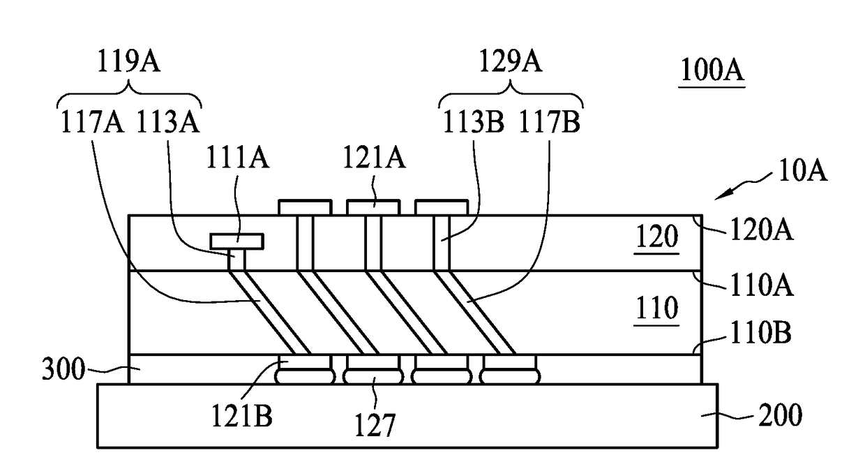
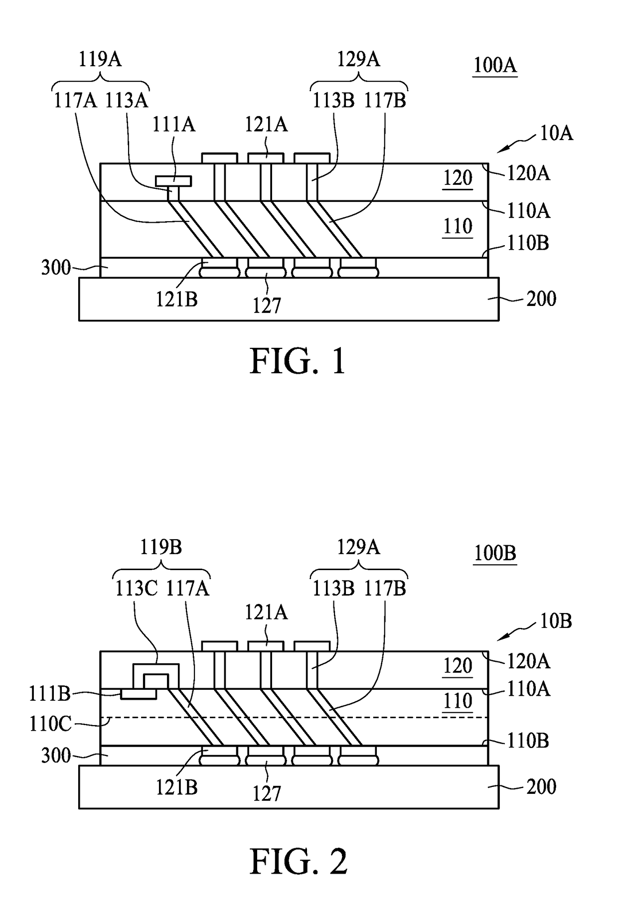
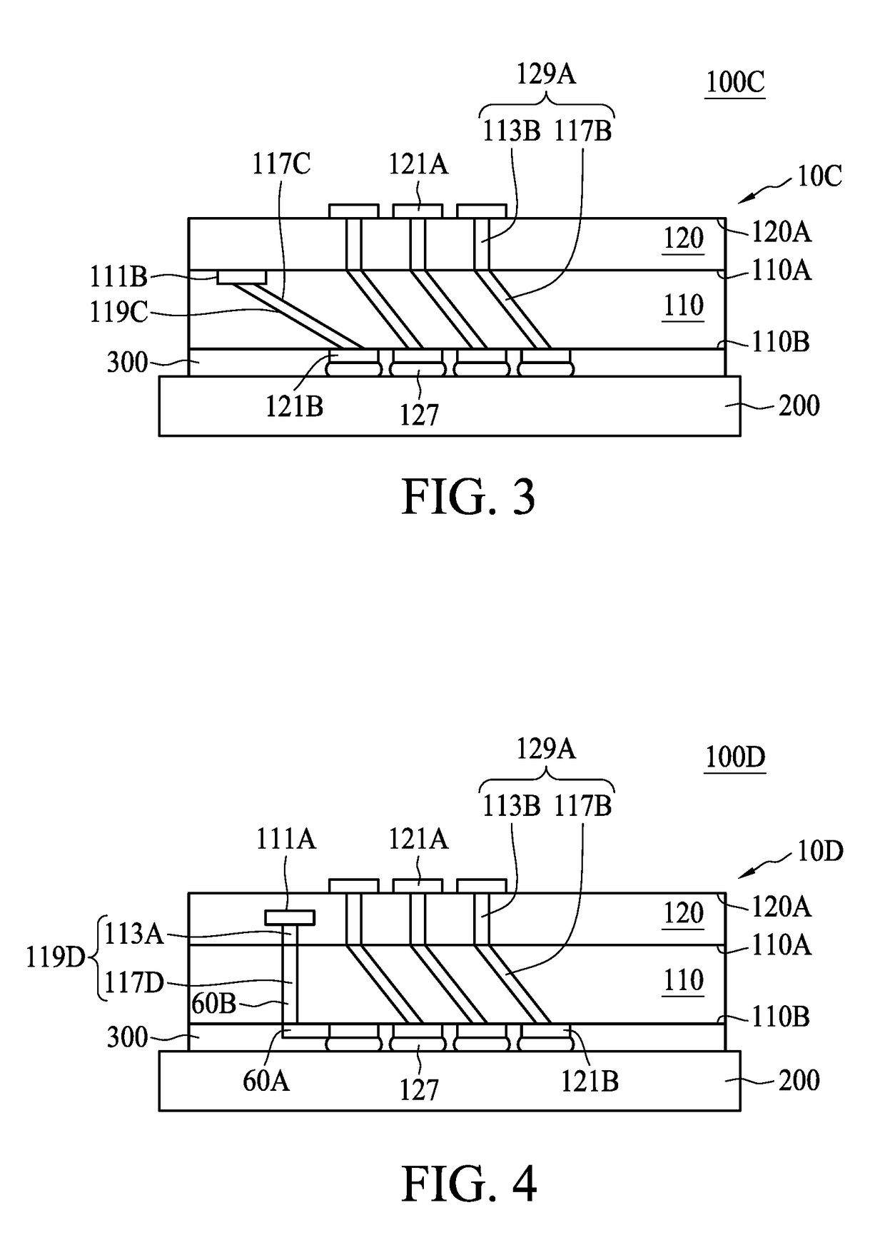
[0048]The present disclosure is directed to a chip package including at least one integrated circuit die having a tilted through silicon via. In order to make the present disclosure co...


PUM


Abstract

A chip package includes at least one integrated circuit die. The integrated circuit die includes a substrate portion having an internal plane between a front side and a back side, an electrical interconnect portion on the front side, a plurality of first connection terminals on an upper surface of the electrical interconnect portion, a plurality of second connection terminals on the back side of the substrate portion, a plurality of connection wirings electrically connecting the first connection terminals and the second connection terminals, a chip selection terminal between the internal plane of the substrate portion and the upper surface of the electrical interconnect portion, and a chip selection wiring connected to the chip selection terminal and one of the second connection terminals and the first connection terminals. At least one of the chip selection wiring and the plurality of connection wirings includes a tilted portion with respect to the back side of the substrate portion.

Description

TECHNICAL FIELD[0001]The present invention relates to a chip package including at least one integrated circuit die having a tilted through silicon via.DISCUSSION OF THE BACKGROUND[0002]Chip stacking technology can bring two chips close together, thereby enabling faster data transmission between the two chips and consuming less power. Memory chips can be stacked together to obtain a memory module with a large storage capacity. In addition to stacking two of the same chip, two chips with different functions may also be stacked together to combine different functions.[0003]In a memory chip stack, each memory chip has a chip selection (CS) terminal, which is used to enable the memory chip. For example, a DRAM chip can have a row address strobe (RAS), column address strobe (CAS), or chip selection pin (CSP) as a chip selection terminal. When a signal is applied to the chip selection terminal of a chip in a memory chip stack, the chip can be accessed, while other chips cannot.[0004]Conven...

Claims


Application Information

Patent Timeline
IPC IPC(8): H01L23/48H01L25/065H01L23/498H01L21/768
CPCH01L23/481H01L21/76898H01L21/76897H01L2225/06548H01L25/0657H01L23/49827H01L2225/06544H01L21/76816H01L23/5384H01L23/5386H01L2224/16145H01L2224/73204H01L2924/15311H01L23/5385H01L2225/06517H01L2225/06513H01L25/18H01L2225/06565H01L2225/06527G11C5/025H01L2924/00014H01L2224/16225H01L2924/181H01L2924/1436H01L2924/14H01L2924/1434H01L2224/06181H01L2224/32225H01L2224/8385H01L2224/83851H01L2924/15788H01L2924/10253H01L2924/10272H01L2924/10271H01L2224/131H01L2224/2929H01L2224/2919H01L2224/0401H01L2224/0557H01L24/05H01L24/06H01L24/13H01L24/32H01L24/16H01L24/73H01L24/09H01L24/17H01L24/81H01L24/83H01L2224/81191H01L2224/13025H01L2924/00012H01L2224/13099H01L2224/32145H01L2924/07802H01L24/00
Inventor LIN, PO CHUN
Owner NAN YA TECH
Why Eureka
Try Eureka