Frame packaging structure integrating passive device and manufacturing method thereof

A technology that integrates passive devices and packaging structures, and is used in semiconductor/solid-state device manufacturing, electrical solid-state devices, semiconductor devices, etc.

Active Publication Date: 2017-07-07
SANECHIPS TECH CO LTD
View PDF3 Cites 1 Cited by
  • Summary
  • Abstract
  • Description
  • Claims
  • Application Information

AI Technical Summary

Problems solved by technology

However, in many cases, the existing frame packages are connected to discrete passive devices through circuit board traces in the system, resulting in a very low...

Method used


Image

  • Frame packaging structure integrating passive device and manufacturing method thereof
  • Frame packaging structure integrating passive device and manufacturing method thereof
  • Frame packaging structure integrating passive device and manufacturing method thereof

Examples


preparation example Construction

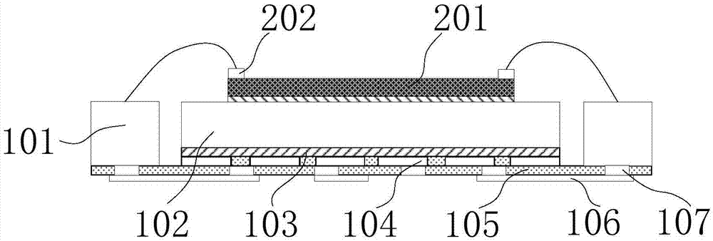
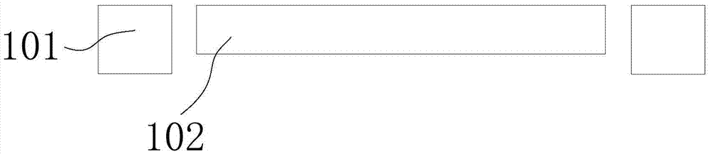
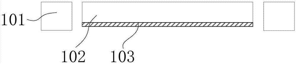
[0050] The method for preparing the frame package structure of integrated passive devices according to the embodiment of the present invention includes the following steps:

[0051] Step 1, providing a lead frame, which includes a die pad and a conductive pad located on the periphery of the die pad;

[0052] Step 2, forming a first insulating dielectric layer on the lower surface of the die pad, and the first insulating layer is deposited by chemical vapor deposition CVD, physical vapor deposition PVD and other processes;

[0053] Step 3, forming a layer of metal conductive material on the lower surface of the first insulating dielectric layer through an electroplating process, and then removing unnecessary metal materials through processes such as photolithography and etching processes, thereby forming a metal structure layer, the metal structure The shape of the layer can be a metal plane arranged in an array in the horizontal direction as the lower plate of the capacitive e...


PUM


Abstract

The invention discloses a frame packaging structure integrating a passive device and a manufacturing method thereof. The frame packaging structure integrating the passive device comprises a bare chip pad, a first insulation dielectric layer, a metal structure layer, a second insulation dielectric layer and at least one conductive pad, wherein the first insulation dielectric layer is arranged below the bare chip pad; the metal structure layer is arranged below the first insulation dielectric layer; the second insulation dielectric layer is arranged below the metal structure layer; and the at least one conductive pad is arranged at a periphery of the bare chip pad. The at least one conductive pad is connected to the second insulation dielectric layer. At least one active chip is arranged on the bare chip pad. The at least one active chip is electrically connected to the conductive pad.

Description

technical field [0001] The invention relates to semiconductor chip packaging technology, in particular to a frame packaging structure of integrated passive devices and a preparation method thereof. Background technique [0002] In the semiconductor industry, the production of integrated circuits can be divided into three stages: integrated circuit design, integrated circuit manufacturing and integrated circuit packaging. After the integrated circuit design is completed, it is handed over to the integrated circuit production factory to complete the integrated circuit production. The integrated circuit chip is completed by the steps of wafer production, integrated circuit formation and wafer cutting. After the integrated circuits inside the wafer are fabricated, a plurality of bonding pads are arranged on the wafer, so that chips formed by dicing the wafer can be point-connected to a carrier outside through these bonding pads. The carrier can be a lead frame or a package subs...

Claims


Application Information

Patent Timeline
IPC IPC(8): H01L21/50H01L21/60H01L23/31H01L23/495
CPCH01L21/50H01L23/31H01L23/49506H01L23/4951H01L24/03H01L24/76H01L2021/60015H01L23/495H01L2224/32145H01L2224/48091H01L2224/48137H01L2224/48145H01L2924/00014H01L2924/00012
Inventor 任晓黎孙拓北
Owner SANECHIPS TECH CO LTD
Why Eureka
Try Eureka