Semiconductor module and an electronic system including the same

a technology of semiconductor modules and electronic systems, applied in the field of semiconductor modules, can solve problems such as difficulty in further developing the performance of semiconductor devices, research into single semiconductor chips or semiconductor packages, and the inability to solve the problems of a single semiconductor device on a system, so as to improve cooling efficiency, improve the performance and integration density of a circuit, and reduce the transmission path

Active Publication Date: 2013-06-04
SAMSUNG ELECTRONICS CO LTD
View PDF14 Cites 1 Cited by
  • Summary
  • Abstract
  • Description
  • Claims
  • Application Information

AI Technical Summary

Benefits of technology

[0006]Exemplary embodiments of the present general inventive concept provide a semiconductor module to reduce a signal transmission path between a logic device and a memory device, and to improve cooling efficiency, so that performance and integration density of a circuit can be enhanced.
[0008]Example embodiments of the present general inventive concept also provide an electronic system including a semiconductor module, so that performance and integration density of the system can be improved.

Problems solved by technology

However, research into a single semiconductor chip or semiconductor package may not facilitate solving problems of a semiconductor device on a system level.
That is, future development of the semiconductor technology on the system level may be difficult to envision.
Therefore, there may be a difficulty in further developing the performance of the semiconductor device.

Method used


Image

  • Semiconductor module and an electronic system including the same
  • Semiconductor module and an electronic system including the same
  • Semiconductor module and an electronic system including the same

Examples


Embodiment Construction

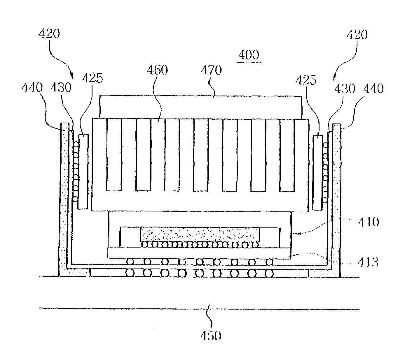
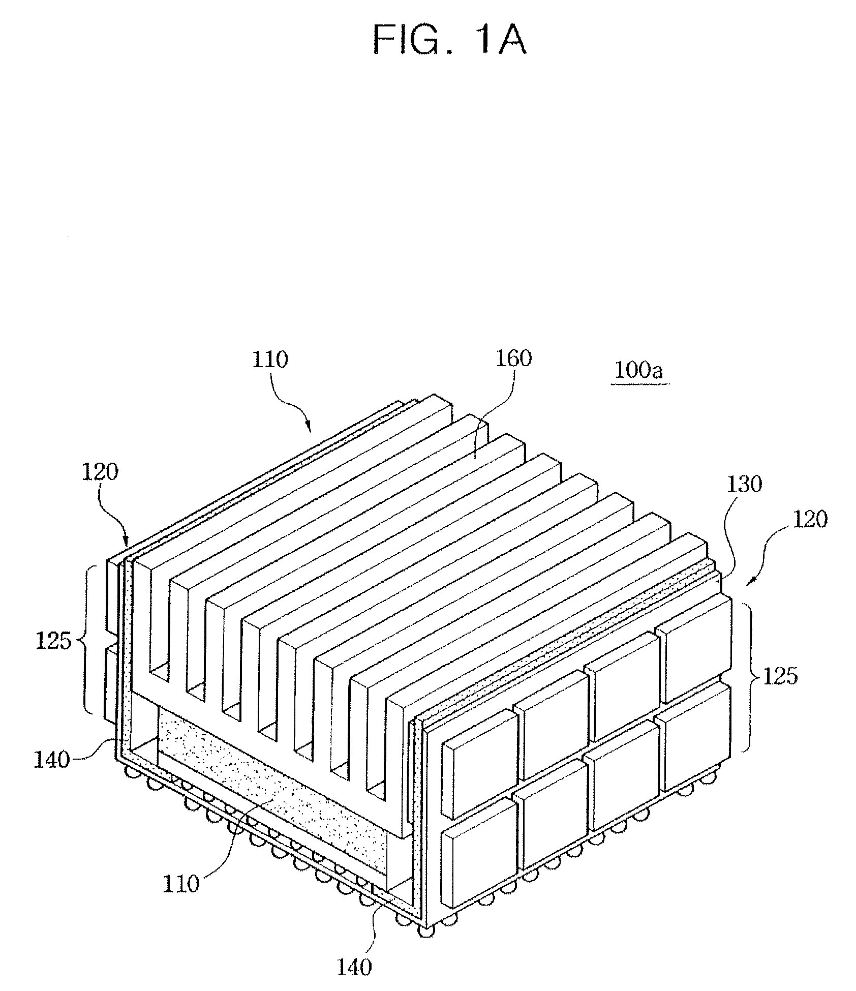
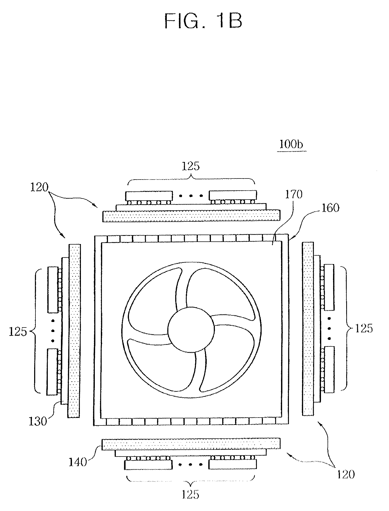
[0021]Various example embodiments will now be described more fully with reference to the accompanying drawings in which example embodiments are illustrated. This inventive concept may, however, be embodied in different forms and should not be construed as limited to the embodiments set forth herein. These embodiments are provided to ensure that this disclosure is thorough and fully enables those skilled in the art to embody and practice the inventive concept. In the drawings, the thicknesses of layers and regions may be exaggerated for clarity. It will also be understood that when a layer is referred to as being “on” another layer or substrate, it can be directly on the other layer or substrate or intervening layers may also be present. Throughout the drawings, like elements are denoted by like reference numerals.

[0022]Example embodiments of the present general inventive concept will be described with reference to plan views and cross-sectional views illustrating the present general...


PUM


Abstract

A three-dimensional semiconductor module and an electronic system including the same are provided. The semiconductor module includes a module substrate, a logic device formed on a part of the module substrate, and a plurality of memory devices formed on another part of the module substrate, wherein the plurality of memory devices are disposed perpendicular to the logic device, and the module substrate on which the plurality of memory devices are formed is supported by a supporter. The electronic system includes the semiconductor module.

Description

CROSS-REFERENCE TO RELATED APPLICATIONS[0001]This application claims priority under 35 U.S.C. §119(a) from Korean Patent Application No. 10-2008-0088880, filed Sep. 9, 2008, the contents of which are hereby incorporated herein by reference in their entirety.BACKGROUND[0002]1. Field of the Invention[0003]The present general inventive concept relates to a semiconductor module, and, in particular, to a semiconductor module including a logic device and a memory device, and an electronic system including the same.[0004]2. Description of the Related Art[0005]Some universally accepted aspects about the development of next generation semiconductor devices include that they will be high in speed, compact in size, low in power consumption, and large in capacity. Along those lines, a multi chip package (MCP) has been receiving remarkable attention together with a system in a package (SIP). These techniques are being researched because they do not significantly depart from conventional semicond...

Claims


Application Information

Patent Timeline
Patent Type & Authority Patents(United States)
IPC IPC(8): H01L23/02H02B1/00H05K7/00H01L23/34H01L23/12H01L23/053H05K1/14H05K1/11H05K1/18H05K1/00H01L23/04
CPCH01L23/467H01L25/18H05K1/147H05K1/189H01L23/5385H01L2225/06579H01L2225/06589H01L2924/09701H01L2924/15311H01L2924/16152H01L2924/3011H05K1/141H05K1/144H05K3/0061H05K2201/046H05K2201/056H05K2201/10159H05K2201/10734H01L2224/16225H01L2224/73253H01L2924/16251H01L2924/00011H01L2924/00014H01L2224/0401H01L23/34H01L23/36H01L23/50
Inventor BAEK, JOONG-HYUN
Owner SAMSUNG ELECTRONICS CO LTD
Why Eureka
Try Eureka