Switching circuit

Inactive Publication Date: 2017-09-14
TOYOTA JIDOSHA KK
View PDF4 Cites 0 Cited by
  • Summary
  • Abstract
  • Description
  • Claims
  • Application Information

AI Technical Summary

Benefits of technology

The patent describes a circuit that controls the switching of a main MOSFET using a control MOSFET. By controlling the signal potential, the circuit can turn on or off the main MOSFET to achieve the desired switching operation. The circuit prevents the low signal potential from affecting the main MOSFET and prevents the change in gate threshold value. The technical effects of this circuit make it possible to achieve effective and reliable switching of the main MOSFET.

Problems solved by technology

A change in the gate threshold value makes it impossible to operate the MOSFET as intended, thus posing a problem.

Method used


Image

  • Switching circuit
  • Switching circuit
  • Switching circuit

Examples


first embodiment

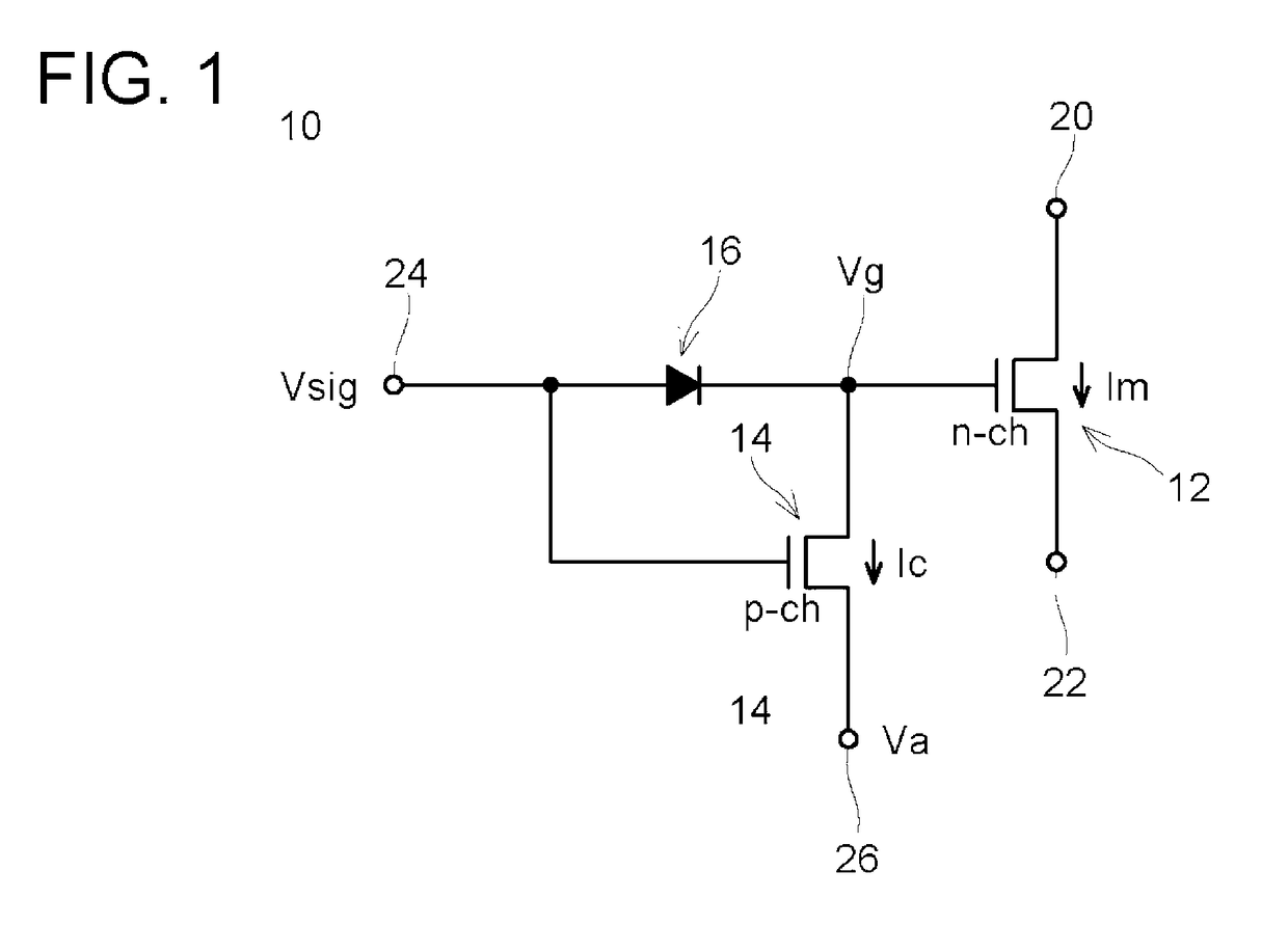
[0019]FIG. 1 shows a switching circuit 10 of the first embodiment. The switching circuit 10 includes a main MOSFET 12, a control MOSFET 14, and a diode 16.

[0020]The main MOSFET 12 is a MOSFET of an n-channel type. A drain of the main MOSFET 12 is connected to a high-potential wire 20, and a source of the main MOSFET 12 is connected to a low-potential wire 22. The main MOSFET 12 is a MOSFET formed in a SiC substrate. More particularly, the main MOSFET 12 includes an n-type source region, a p-type body region, and an n-type drain region, all of which are formed in the SiC substrate. Further, a gate insulator film (silicon oxide film) is in contact with the body region. A gate electrode faces the body region via the gate insulator film. The application of a potential that is equal to or higher than a threshold value to the gate electrode forms an n-type channel in the body region, so that the source region and the drain region are connected to each other through the channel. The main M...

second embodiment

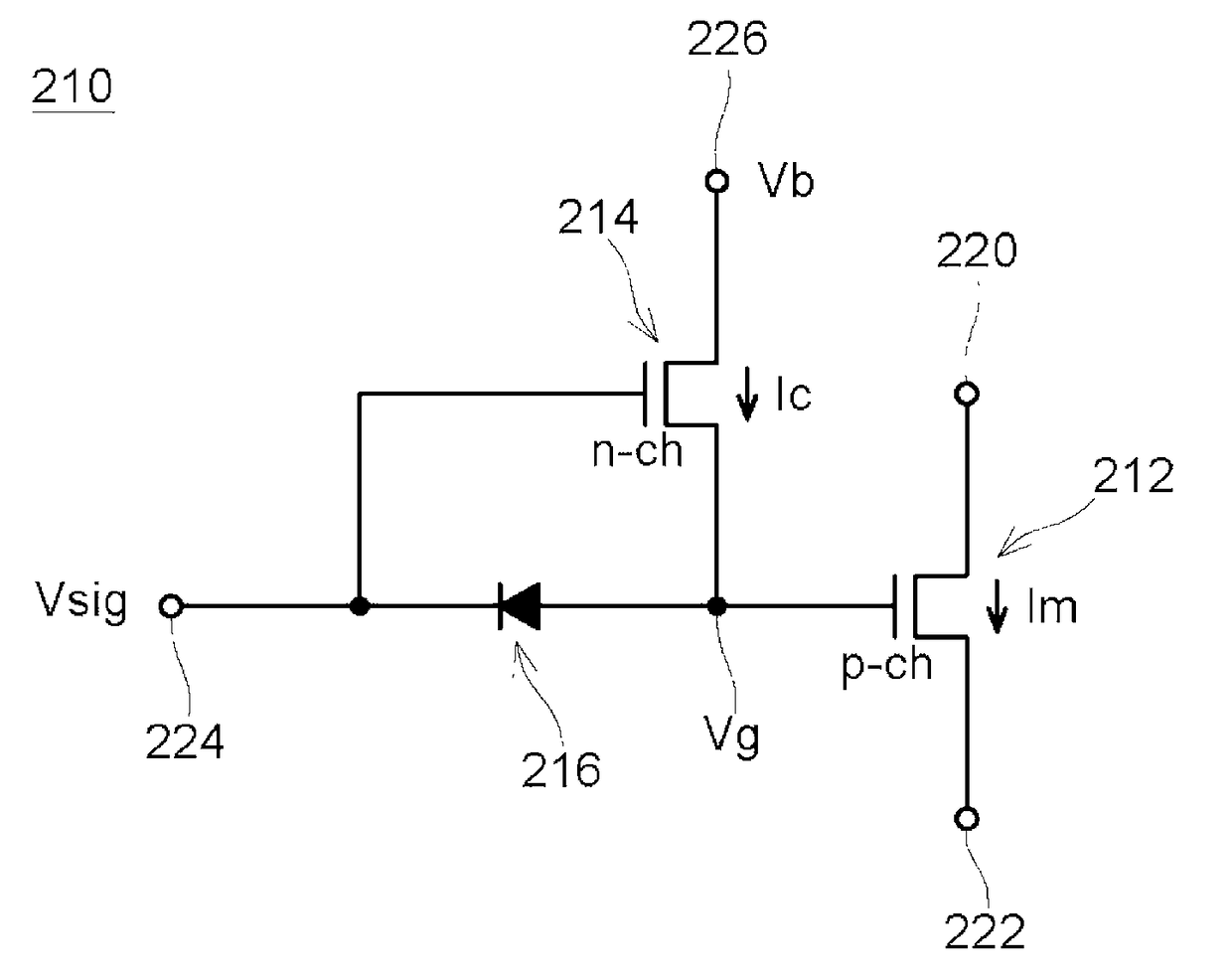
[0032]FIG. 8 shows a switching circuit 210 of the second embodiment. The switching circuit 210 includes a main MOSFET 212 of the p-channel type and a control MOSFET 214 of the n-channel type. A configuration of the switching circuit 210 of the second embodiment will be described in detail below.

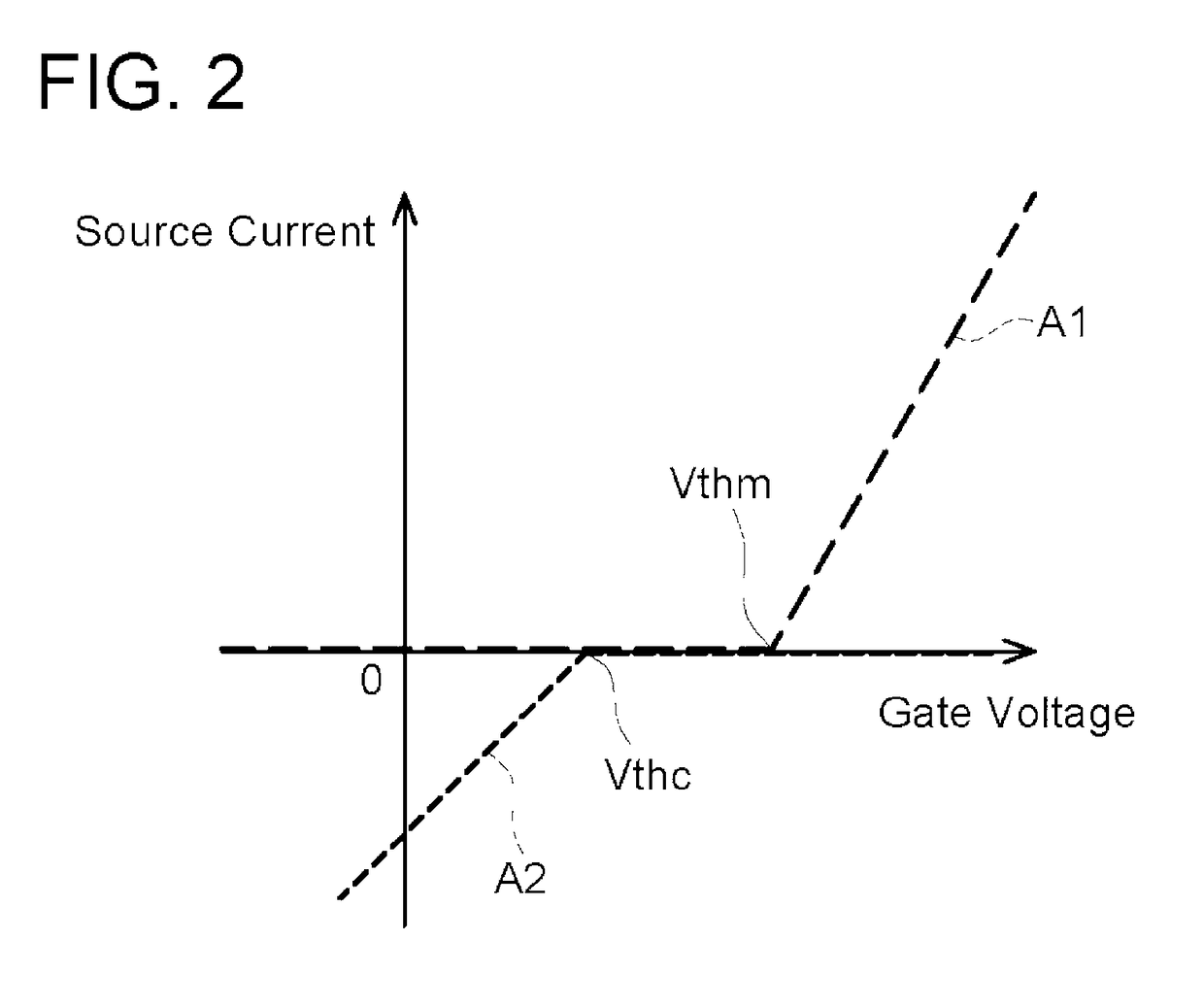
[0033]The main MOSFET 212 is a MOSFET of the p-channel type. A source of the main MOSFET 212 is connected to a high-potential wire 220, and a drain of the main MOSFET 212 is connected to a low-potential wire 222. The main MOSFET 212 is a MOSFET formed in a SiC substrate. The main MOSFET 212 is turned on when a potential that is equal to or lower than a threshold value Vthm is applied to a gate of the main MOSFET 212.

[0034]The control MOSFET 214 is a MOSFET of the n-channel type. A source of the control MOSFET 214 is connected to the gate of the main MOSFET 212. A drain of the control MOSFET 214 is connected to a positive wire 226. A gate of the control MOSFET 214 is connected to a signal wire...


PUM


Abstract

A switching circuit disclosed, herein, includes a main MOSFET 12, a control MOSFET 14, and a diode 16. The main MOSFET is formed in a SiC semiconductor layer. A channel type of the main MOSFET is a first conductivity type. A channel type of the control MOSFET is a second conductivity type. A source of the control MOSFET is connected to-a gate of the main MOS-FET. A cathode of the diode is connected to a gate of one of the main MOSFET and the control MOSFET. An anode of the diode is connected to a gate of the other of the main MOSFET and the control MOSFET. A channel type of the one is an n-type. A channel type of the other is a p-type.

Description

TECHNICAL FIELDCROSS-REFERENCE TO RELATED APPLICATION[0001]This application claims priority to Japanese Patent Application No. 2014-209138 filed on Oct. 10, 2014, the contents of which are hereby incorporated by reference into the present application.[0002]A technology disclosed herein relates to a switching circuit.BACKGROUND ART[0003]Japanese Patent Application Publication No. 2012-54378 discloses a MOSFET. Further, in recent years, SiC has been used as a semiconductor material for a MOSFET in some cases.SUMMARY OF INVENTION[0004]It has been known that in a MOSFET formed in a SiC semiconductor layer, an application of an inappropriate potential to a gate of the MOSFET changes a gate threshold value. For example, in a MOSFET of an n-channel type, the application of a negative potential that is lower than a predetermined value to a gate of the MOSFET changes the gate threshold value toward a negative side. Alternatively, in a MOSFET of a p-channel type, the application of a positive...

Claims


Application Information

Patent Timeline
IPC IPC(8): H03K17/0812H01L27/02H01L27/06H01L29/16H01L29/78
CPCH03K17/08122H01L29/1608H01L27/0285H01L27/0629H01L29/16H01L29/78
Inventor SUGIMOTO, MASAHIROWATANABE, YUKIHIKOYAMAMOTO, KENSAKU
Owner TOYOTA JIDOSHA KK
Why Eureka
Try Eureka