Passive device assembly for accurate ground plane control

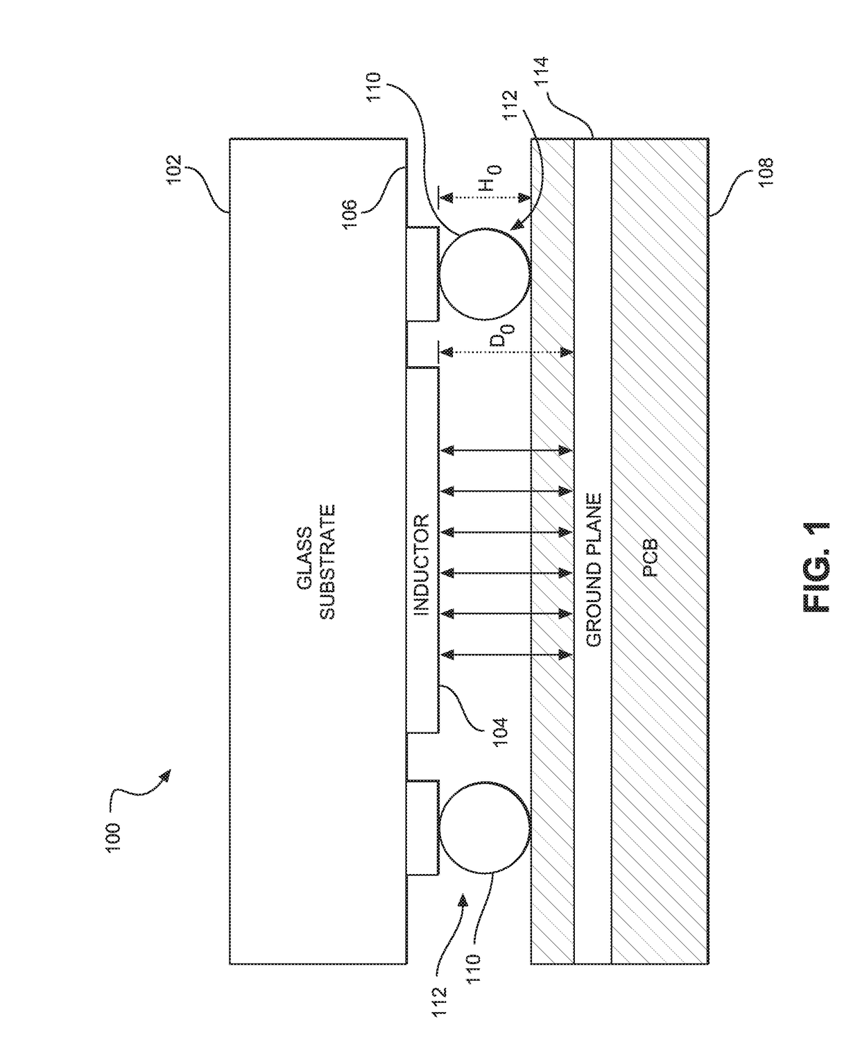
a passive device and ground plane control technology, applied in the direction of printed element electric connection formation, association of printed circuit non-printed electric components, conductive pattern formation, etc., can solve the problem of difficult to achieve a desired and consistent height, high risk of reflow degradation, and the separation distance dsub>0 /sub>to vary (e.g., decrease), and achieve accurate control. , the effect of minimizing or eliminating undesirable inductance interferen

Inactive Publication Date: 2017-09-28
QUALCOMM INC
View PDF4 Cites 3 Cited by
  • Summary
  • Abstract
  • Description
  • Claims
  • Application Information

AI Technical Summary

Benefits of technology

[0007]Aspects disclosed herein include passive device assembly for accurate ground plane control. In one aspect, a passive device assembly is provided that includes a passive device(s) (e.g., an inductor(s) and / or a capacitor(s)) for use in a circuit, such as a radio-frequency (RF) filter for example. The passive device assembly includes a device substrate and a ground plane separation control substrate. The device substrate is disposed above and conductively coupled to the ground plane separation control substrate. A passive device(s) disposed on a lower surface of the device substrate is separated from an embedded ground plane mounted on a lower surface of the ground plane separation control substrate by a separation distance. The separation distance is accurately controlled by controlling the height of the ground plane separation control substrate to minimize or eliminate undesirable inductance interference that may occur between the passive device(s) and the embedded ground plane. In this manner, the separation distance is controlled by structures that are contained with the passive device assembly. In another aspect, conductive mounting pads are disposed on the lower surface of the ground plane separation control substrate to support accurate alignment of the passive device assembly on a circuit board. By providing sufficient separation distance inside the passive device assembly to minimize undesirable inductance interference that may occur between the passive device(s) and the embedded ground plane, the passive device assembly can be precisely mounted onto any circuit board regardless of specific design and layout of the circuit board.

Problems solved by technology

However, it may be difficult to achieve a desired and consistent height H0 of the solder balls 110 that form the BGAs 112.
In addition, the solder balls 110 may also tend to be highly susceptible to reflow degradation, which can cause the separation distance D0 to vary (e.g., decrease), as a result.
Furthermore, over the course of operation, the reflow degeneration of the solder balls 110 may lead to collapse of the 2D POG structure in the conventional semiconductor package 100 due to high heat and stress that is common in semiconductor packages like the conventional semiconductor package 100.

Method used


Image

  • Passive device assembly for accurate ground plane control
  • Passive device assembly for accurate ground plane control
  • Passive device assembly for accurate ground plane control

Examples


Embodiment Construction

[0019]With reference now to the drawing figures, several exemplary aspects of the present disclosure are described. The word “exemplary” is used herein to mean “serving as an example, instance, or illustration.” Any aspect described herein as “exemplary” is not necessarily to be construed as preferred or advantageous over other aspects.

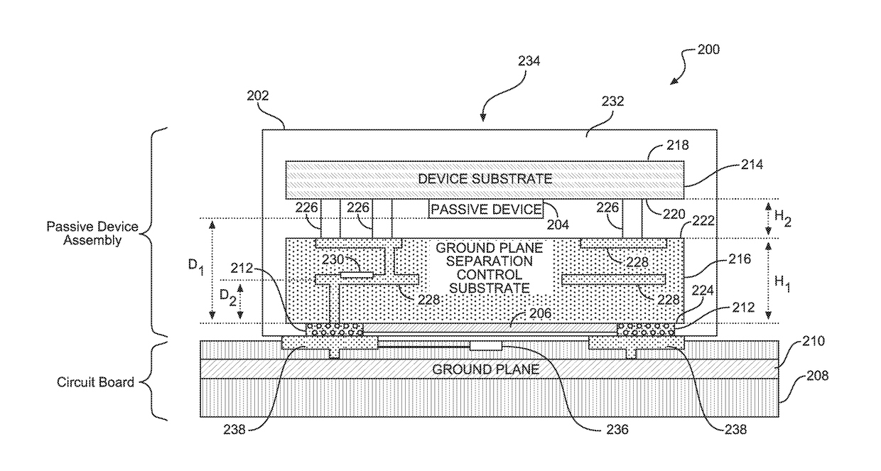
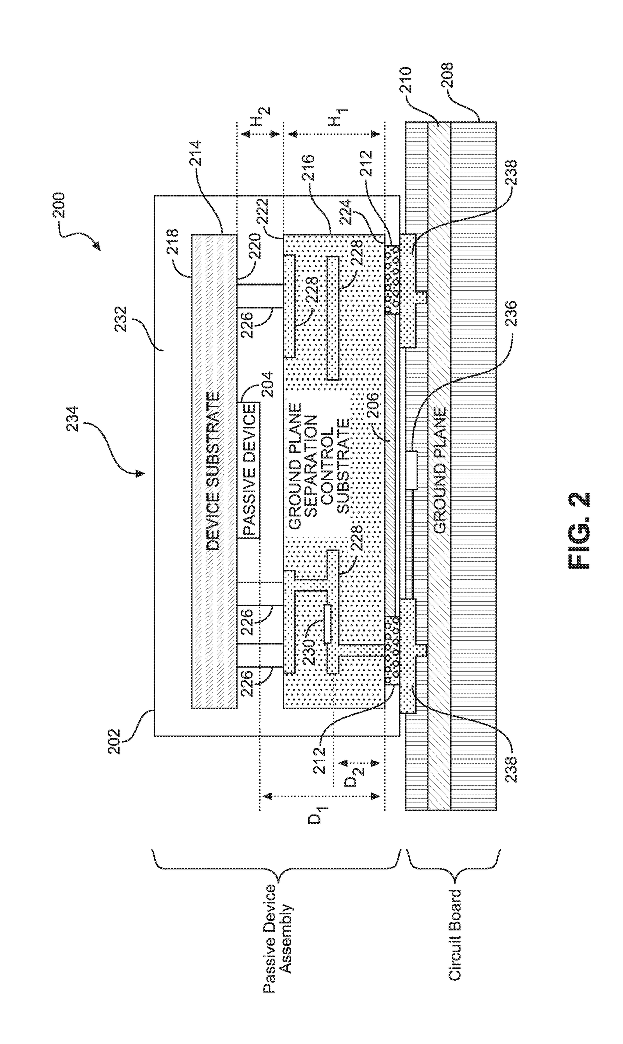
[0020]Aspects disclosed herein include passive device assembly for accurate ground plane control. In one aspect, a passive device assembly is provided that includes a passive device(s) (e.g., an inductor(s) and / or a capacitor(s)) for use in a circuit, such as a radio-frequency (RF) filter for example. The passive device assembly includes a device substrate and a ground plane separation control substrate. The device substrate is disposed above and conductively coupled to the ground plane separation control substrate. A passive device(s) disposed on a lower surface of the device substrate is separated from an embedded ground plane mounted on a lower sur...


PUM


Abstract

Passive device assembly for accurate ground plane control is disclosed. A passive device assembly includes a device substrate conductively coupled to a ground plane separation control substrate. A passive device disposed on a lower surface of the device substrate is separated from an embedded ground plane mounted on a lower surface of the ground plane separation control substrate by a separation distance. The separation distance is accurately controlled to minimize undesirable interference that may occur to the passive device. The separation distance is provided inside the passive device assembly. Conductive mounting pads are disposed on the lower surface of the ground plane separation control substrate to support accurate alignment of the passive device assembly on a circuit board. By providing sufficient separation distance inside the passive device assembly, the passive device assembly can be precisely mounted onto any circuit board regardless of specific design and layout of the circuit board.

Description

BACKGROUND[0001]I. Field of the Disclosure[0002]The technology of the disclosure relates generally to semiconductor packaging of semiconductor dies and passive components, and more specifically to minimizing undesirable inductance interference between the passive components and a ground plane of circuit board to which the semiconductor package is mounted.[0003]II. Background[0004]Semiconductor packages typically involve one or more semiconductor dies integrated on a substrate, such as a glass substrate. The substrate is then attached to a package base, such as a printed circuit board (PCB). Passive components such as capacitors and inductors are usually formed on one side, such as a lower side, of the substrate. The substrate may be attached to the PCB, face down, such that the lower side having the passive components is closest to the PCB. Ball grid arrays (BGAs) including solder balls may be utilized for forming the connections and attachment between the substrate and the PCB. Ele...

Claims


Application Information

Patent Timeline
Patent Type & Authority Applications(United States)
IPC IPC(8): H05K1/18H05K3/10H05K3/40H03H7/01H05K3/30
CPCH05K1/181H03H7/0138H05K3/10H05K3/4007H05K3/303H01L23/552H05K1/0218H05K1/141H05K2201/042H05K2201/045H05K2201/1003H05K2201/10098H05K2201/10962H05K2201/2036H01L23/3107H01L21/56H01L23/12H01L23/15H01L23/28H05K2201/09227H01L23/5386H01L23/5389
Inventor ZUO, CHENGJIEBERDY, DAVID FRANCISKIM, DAEIK DANIELYUN, CHANGHAN HOBIEVELEZ, MARIO FRANCISCOKIM, JONGHAE
Owner QUALCOMM INC
Why Eureka
Try Eureka