
Method and circuit for self-training of a reference voltage and memory system including the same

a reference voltage and memory system technology, applied in the field of semiconductor integrated circuits, can solve problems such as system performance degradation, and achieve the effects of efficiently providing a reference voltag

Active Publication Date: 2017-10-05
SAMSUNG ELECTRONICS CO LTD
View PDF0 Cites 15 Cited by
  • Summary
  • Abstract
  • Description
  • Claims
  • Application Information

AI Technical Summary

Benefits of technology

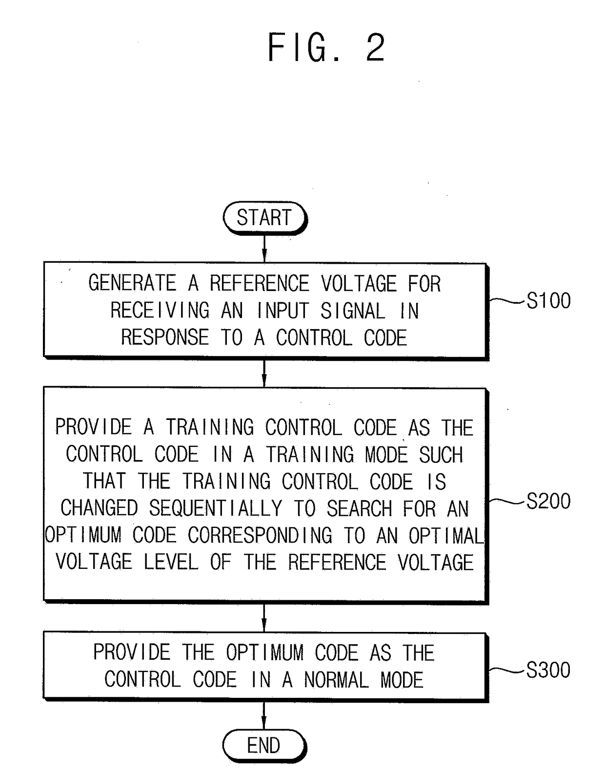
The patent text describes a circuit and method for efficiently providing a reference voltage for a reception interface. This may be useful in a memory system or package. The technical effect of this patent is to improve the accuracy and reliability of reference voltage in a memory system.

Problems solved by technology

If the voltage level of the reference voltage is improper or inaccurate, errors may increase in determining the logic levels of the received signals and thus performance of the system may be degraded.

Method used


Image

  • Method and circuit for self-training of a reference voltage and memory system including the same
  • Method and circuit for self-training of a reference voltage and memory system including the same
  • Method and circuit for self-training of a reference voltage and memory system including the same

Examples


Embodiment Construction

[0032]The present disclosure now will be described more fully hereinafter with reference to the accompanying drawings, in which various embodiments are shown. The invention may, however, be embodied in many different forms and should not be construed as limited to the example embodiments set forth herein. These example embodiments are just that—examples—and many implementations and variations are possible that do not require the details provided herein. It should also be emphasized that the disclosure provides details of alternative examples, but such listing of alternatives is not exhaustive. Furthermore, any consistency of detail between various examples should not be interpreted as requiring such detail—it is impracticable to list every possible variation for every feature described herein. The language of the claims should be referenced in determining the requirements of the invention.

[0033]In the drawings, like numbers refer to like elements throughout. Though the different fig...


PUM


Abstract

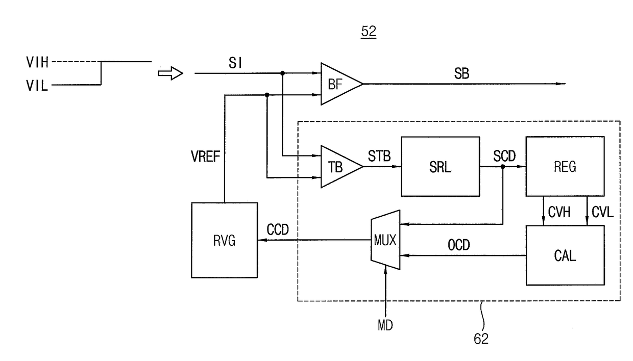
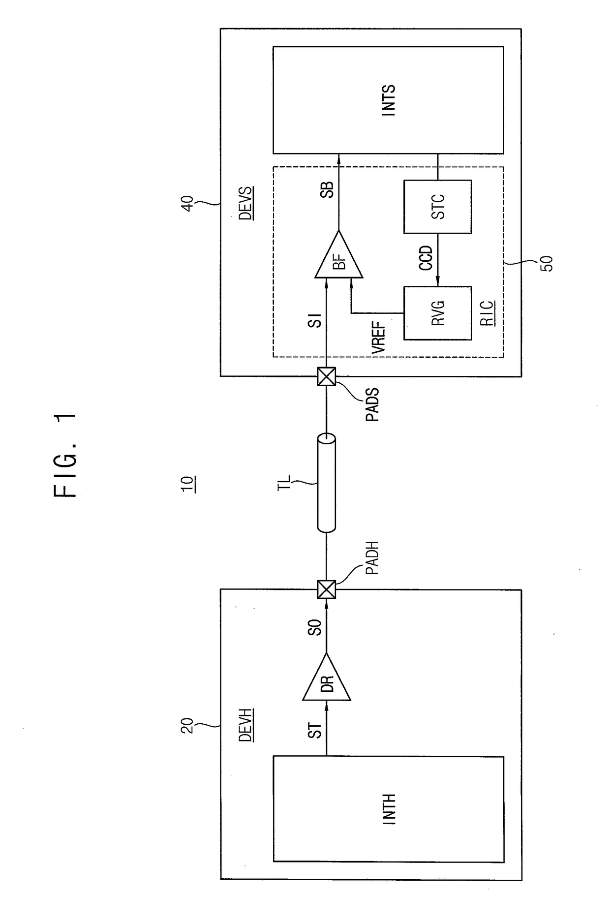
A semiconductor device, includes at least a first memory chip, which includes at least a first buffer connected to receive an input signal and a reference voltage; at least a first reference voltage generator configured to output a reference voltage based on a first control code; and at least a first self-training circuit for determining an operational reference voltage to use during a normal mode of operation of the semiconductor device. An output from the first buffer is input to the first self-training circuit, the first control code is output from the first self-training circuit into the first reference voltage generator, and the first buffer, the first self-training circuit, and the first reference voltage generator form a loop.

Description

CROSS-REFERENCE TO RELATED APPLICATION[0001]This U.S. Non-provisional application claims priority under 35 USC §119 to Korean Patent Application No. 10-2016-0039099, filed on Mar. 31, 2016, in the Korean Intellectual Property Office (KIPO), the disclosure of which is incorporated by reference in its entirety herein.BACKGROUND1. Technical Field[0002]Example embodiments relate generally to semiconductor integrated circuits, and more particularly to a method and circuit for self-training of a reference voltage, and a memory system including the circuit.2. Discussion of the Related Art[0003]In comparison with a semiconductor device receiving a differential signal, a semiconductor device receiving a single-ended signal typically requires a reference voltage for determining a logic level of a received signal. It is desirable to set the voltage level of the reference voltage to a mean value of the low voltage level and the high voltage level of the received signal.[0004]A semiconductor dev...

Claims


Application Information

Patent Timeline
IPC IPC(8): G11C7/14G11C7/10
CPCG11C7/1057G11C7/14G11C5/147G11C7/1084G11C29/021G11C29/028G11C29/4401G11C7/1078G11C7/1006
Inventor LEE, SEON-KYOOIHM, JEONG-DONJEONG, BYUNG-HOONKANG, DAE-WOON
Owner SAMSUNG ELECTRONICS CO LTD
Learn More