Near-field communication (NFC) system and method for high performance NFC and wireless power transfer with small antennas
- Summary
- Abstract
- Description
- Claims
- Application Information
AI Technical Summary
Benefits of technology
Problems solved by technology
Method used
Image

Examples
first embodiment
[0065 of NFC Tag
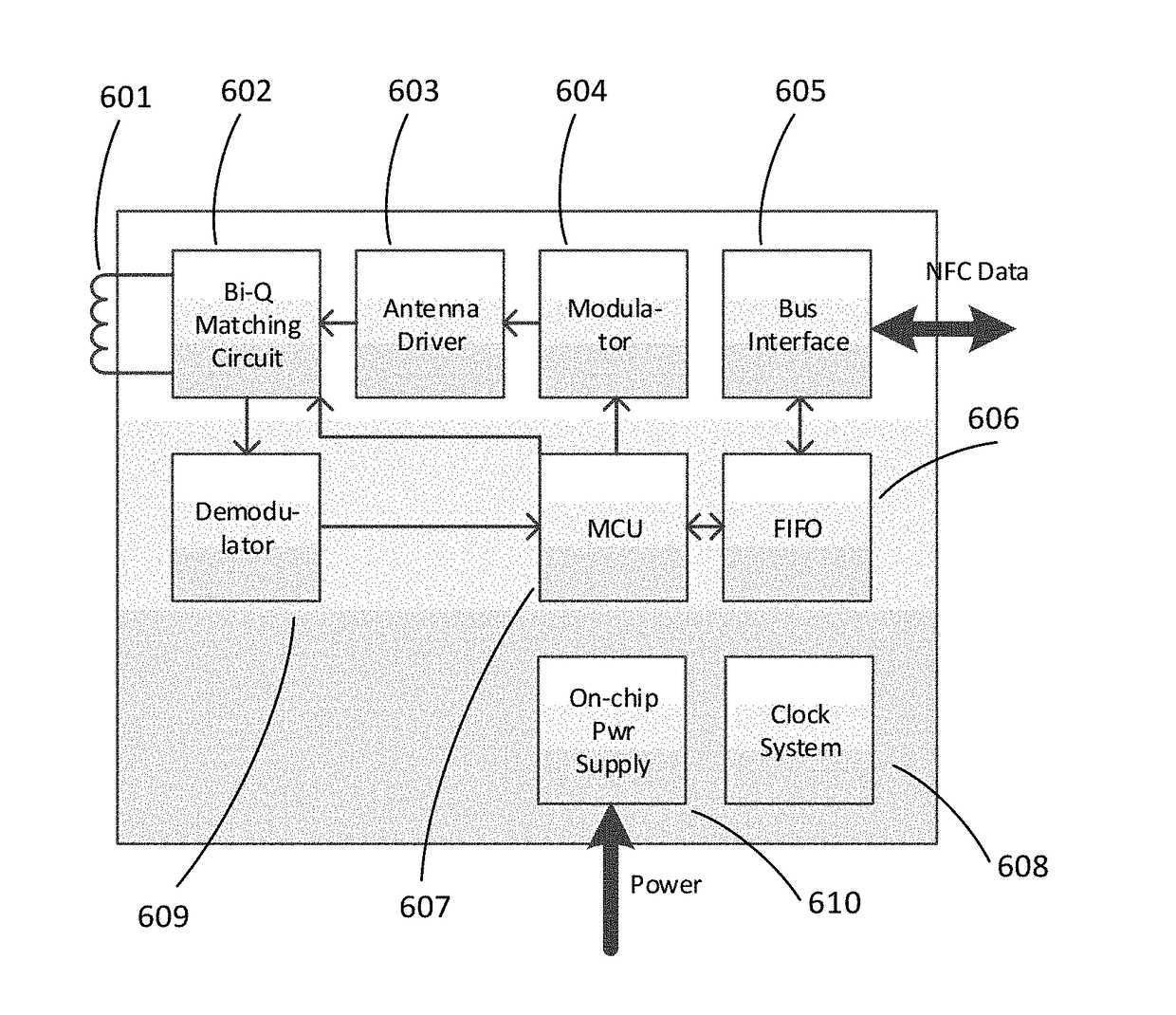
[0066]FIG. 9 shows the architecture of a NFC tag interface in one embodiment of the invention. Antenna 901 is a loop antenna with a high Q, which receives the wireless power and NFC signals transmitted by a nearby NFC reader, as well as transmits NFC signals. Bi-Q Matching Circuit 902 adjusts the impedance of Antenna 901 to a proper value. It has two working modes, i.e., a high-Q mode and a low-Q mode, which can tune the Q-factor of the antenna resonant circuit to a high (Q≧50) and low (Q≦25) value, respectively. Demodulator 903 demodulates the NFC signals received by Antenna 901. Load Modulator 905 modulates the load to Antenna 901 in order to transmit the signal. Bus Interface 904 connects to external devices via a system data bus, and is used for exchanging NFC data and configuring the NFC tag interface. Rectifier and Regulator Circuit 906 converts the RF energy that Antenna 901 harvested to a regulated DC power, which could be used for powering the tag interface,...
second embodiment
[0075 of NFC Tag
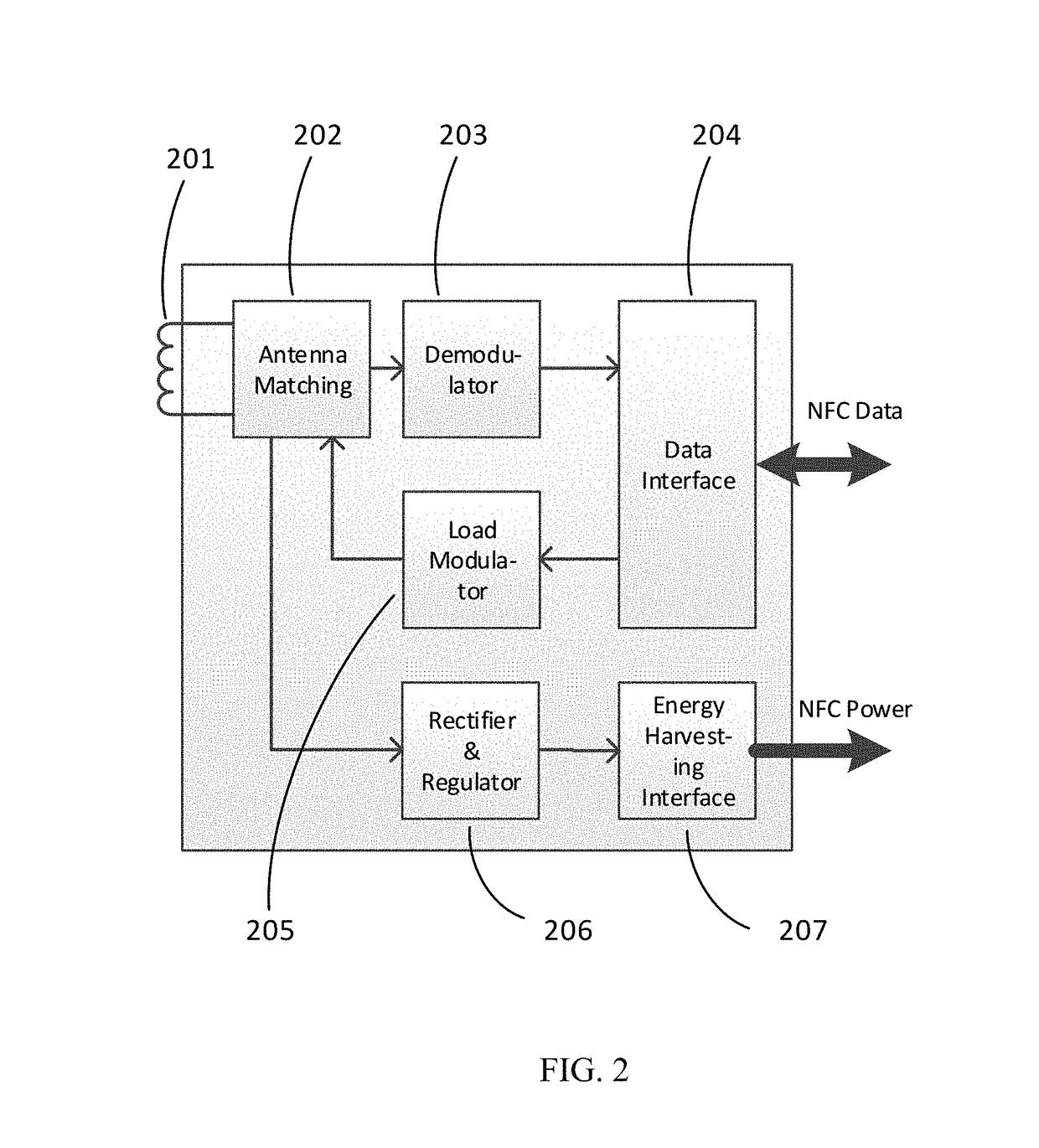
[0076]FIG. 12 shows the architecture of the NFC tag interface in another embodiment of the invention. The disclosed NFC tag design contains two antennas, Antenna 1201 and Antenna 1205, and two antenna resonant circuits. Antenna 1201 and Antenna Matching Circuit 1202 comprise the first antenna resonant circuit with a low Q (Q≦25), which is utilized to receive the NFC signal transmitted by nearby NFC readers. Antenna 1205 and Antenna Matching Circuit 1206 comprise the second antenna resonant circuit with a high Q (Q≧50), which is used to harvest nearby RF energy and perform load modulation. Demodulator 1203 demodulates the signal received by Antenna 1201, and sends the data to Bus Interface 1204, which connects with external devices via a data bus. Load Modulator 1208 modulates the load connected to Antenna 1205 according to the data received from the data bus. Bus Interface 1204 serves as the data exchanging hub for Demodulator 1203, Load Modulator 1208, and external ...
PUM
 Abstract
Description
Claims
Application Information
 - R&D Engineer
- R&D Manager
- IP Professional
- Industry Leading Data Capabilities
- Powerful AI technology
- Patent DNA Extraction
Browse by: Latest US Patents, China's latest patents, Technical Efficacy Thesaurus, Application Domain, Technology Topic.
© 2024 PatSnap. All rights reserved.Legal|Privacy policy|Modern Slavery Act Transparency Statement|Sitemap