RF power amplifier

a power amplifier and power supply technology, applied in the direction of push-pull amplifiers, amplifiers with min 3 electrodes or 2 pn junctions, phase splitters, etc., can solve the problem of unsatisfactory cost, and achieve the effect of reducing the input impedance of the primary side of the transformer

Active Publication Date: 2010-05-13
RENESAS ELECTRONICS CORP
View PDF3 Cites 51 Cited by
  • Summary
  • Abstract
  • Description
  • Claims
  • Application Information

AI Technical Summary

Benefits of technology

[0042]That is, an RF power amplifier can be provided in which the primary-side input impedance of a transformer can be reduced without involving a reduction in Q-factor.

Problems solved by technology

In Non-Patent Document 4 shown below, it is also stated that the power coupling structure of the distributed active-transformer (DAT), which is rather large compared with active devices, determines the total chip size, and hence is not desirable in terms of cost.

Method used


Image

  • RF power amplifier
  • RF power amplifier
  • RF power amplifier

Examples


embodiment

Representative Embodiment

[0061]First, a description will be given of an outline of representative embodiments of the invention disclosed in the present application. Reference numerals in the drawings which are nestled in parentheses and referenced in the description of the outline of the representative embodiments are only illustrative of the content of the concept of the components provided with the reference numerals.

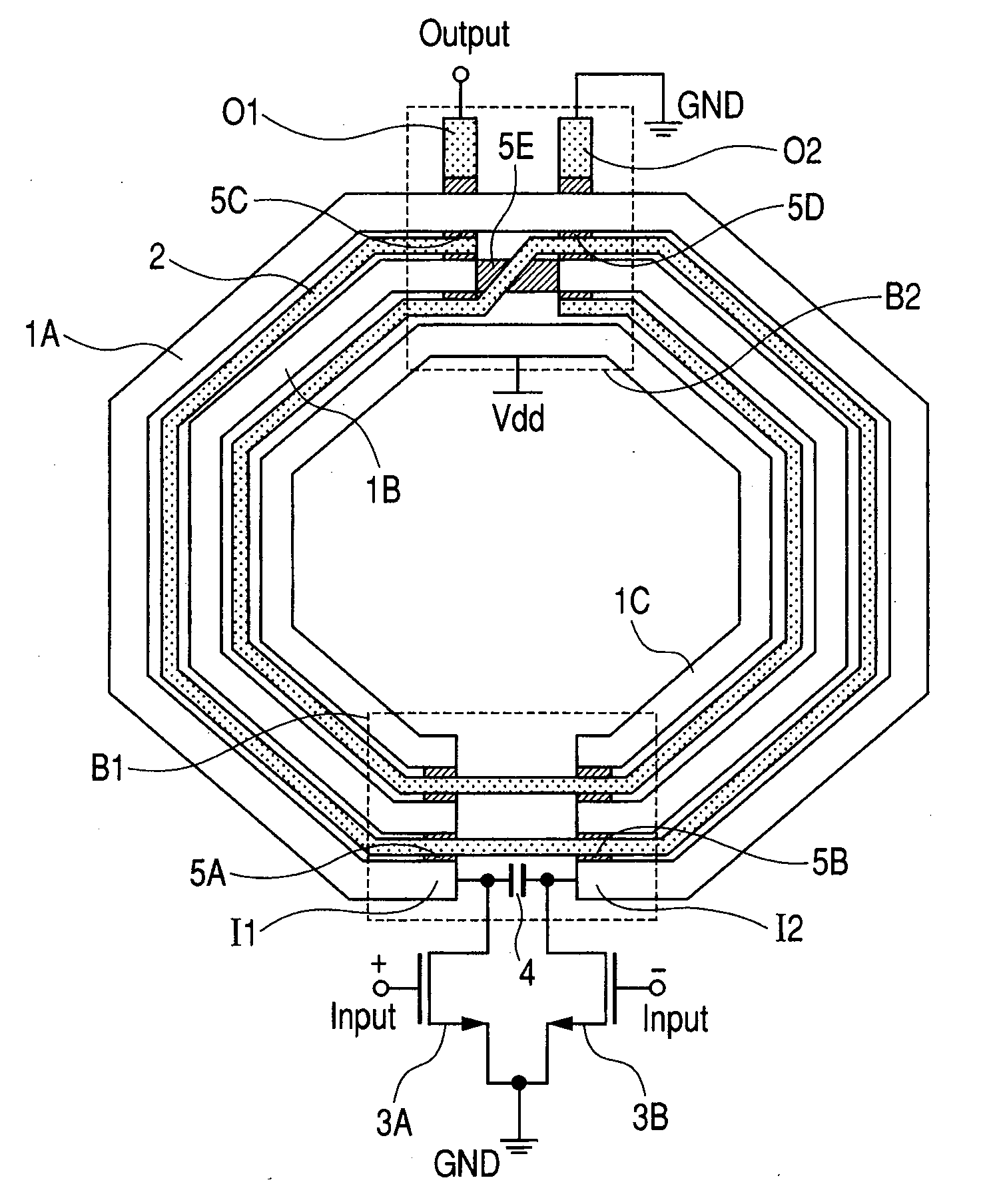
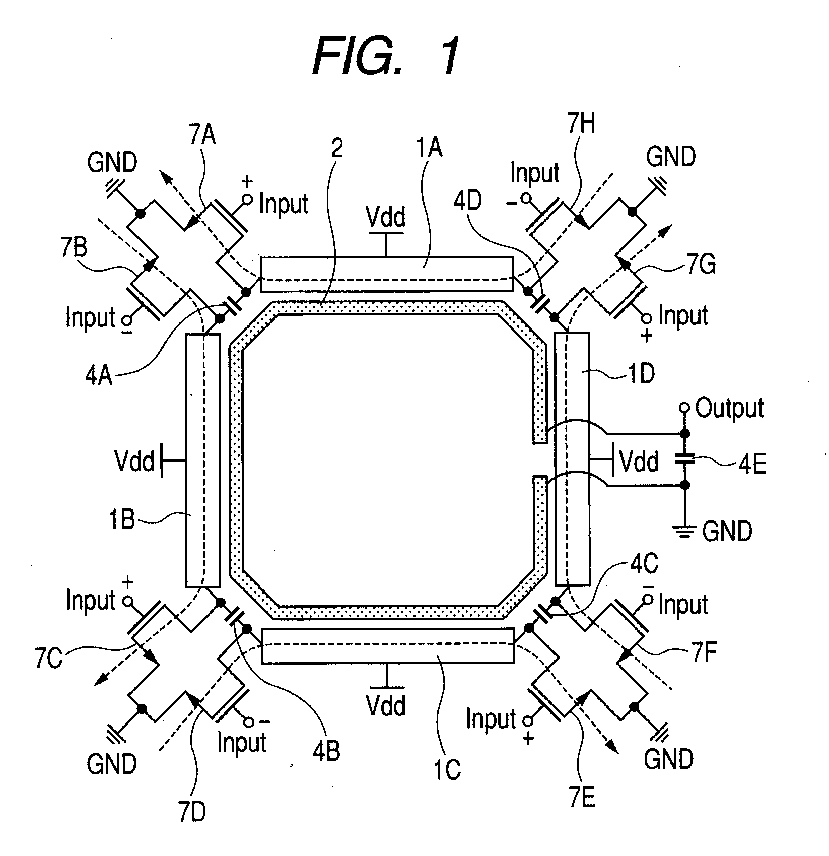
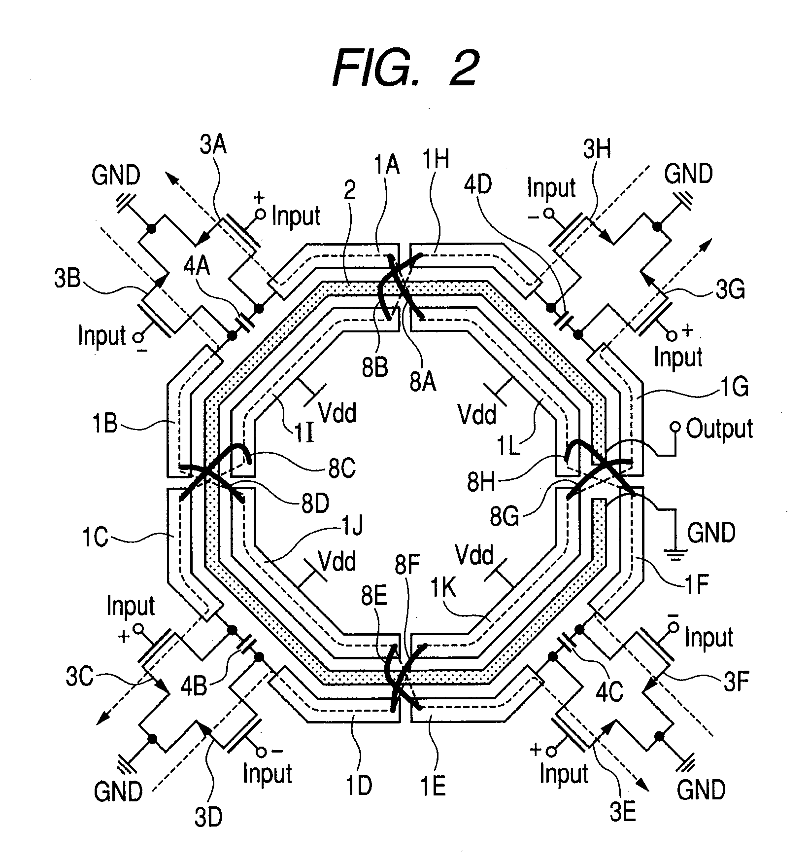
[0062](1) An RF power amplifier according to a representative embodiment of the present invention includes a first transistor (3A) and a second transistor (3B) each as an active device of a push-pull power amplification circuit, and a transformer (1A, 1B, and 2) as an output matching circuit of the push-pull power amplification circuit.

[0063]An input terminal of the first transistor (3A) and an input terminal of the second transistor (3B) can be respectively supplied with a non-inverted input signal (+Input) and an inverted input signal (−Input).

[0064]The transformer ...


PUM


Abstract

A reduction is achieved in the primary-side input impedance of a transformer (voltage transformer) as an output matching circuit without involving a reduction in Q-factor. An RF power amplifier includes transistors, and a transformer as the output matching circuit. The transformer has a primary coil and a secondary coil which are magnetically coupled to each other. To the input terminals of the transistors, respective input signals are supplied. The primary coil is coupled to each of the output terminals of the transistors. From the secondary coil, an output signal is generated. The primary coil includes a first coil and a second coil which are coupled in parallel between the respective output terminals of the transistors, and each magnetically coupled to the secondary coil. By the parallel coupling of the first and second coils of the primary coil, the input impedance of the primary coil is reduced.

Description

CROSS-REFERENCE TO RELATED APPLICATIONS[0001]The disclosure of Japanese Patent Application No. 2008-290911 filed on Nov. 13, 2008 including the specification, drawings and abstract is incorporated herein by reference in its entirety.BACKGROUND OF THE INVENTION[0002]The present invention relates to RF power amplifiers, and particularly to a technology which is effective in reducing the input impedance of a primary coil in a transformer of an impedance matching circuit without involving a reduction in Q-factor.[0003]As has been well known, in a radio-frequency (RF) power amplifier mounted in a communication device such as a mobile phone terminal device or a wireless LAN terminal, an impedance matching circuit is coupled between a source-grounded or emitter-grounded power amplification transistor and a load for the purpose of efficiently driving the antenna of the load with the power amplification transistor. The impedance matching circuit transforms a low output impedance of several o...

Claims


Application Information

Patent Timeline
Patent Type & Authority Applications(United States)
IPC IPC(8): H03F3/26
CPCH03F1/0272H03F3/21H03F3/195H03F3/245H03F3/265H03F3/45179H03F3/45475H03F3/68H03F2200/105H03F2200/222H03F2200/387H03F2200/411H03F2200/451H03F2200/465H03F2200/534H03F2200/541H03F2203/45481H03F2203/45544H03F2203/45621H03F2203/45631H03F2203/45731H03F3/26H03F3/193H03F1/565H01L2224/0603H01L2224/48091H01L2224/48227H01L2224/49111H01L2924/13091H01L2924/00014H01L2924/00
Inventor KONDO, MASAOMATSUNAGA, YOSHIKUNISEKI, KENTASAKURAI, SATOSHI
Owner RENESAS ELECTRONICS CORP
Why Eureka
Try Eureka