Power device with high switching speed and manufacturing method thereof

a technology of power devices and switching speeds, applied in semiconductor devices, basic electric elements, electric devices, etc., can solve the problems of increasing the size of the device, increasing the cost, and limiting their use, and achieves short switching times, low voltage drop, and high input impedance

Active Publication Date: 2007-04-26
STMICROELECTRONICS SRL
View PDF3 Cites 10 Cited by
  • Summary
  • Abstract
  • Description
  • Claims
  • Application Information

AI Technical Summary

Benefits of technology

[0010] The power device according to the invention combines a thyristor structure, and hence has a low voltage drop across its terminals in the on state, with a high input impedance, such as an IGBT. The described power device has very short switching times, comparable with those of a MOSFET, by virtue of a fast removal of charges from t...

Problems solved by technology

Amongst the hybrid solutions proposed, the most versatile solution is the IGBT one, even though its characteristics do not render it suitable for applications requiring a high blocking voltage (maximum reverse voltage that the device is able to withstand without going into breakdown), which is typically higher than 1200 V. In fact, at higher voltages, the power dissipation i...

Method used


Image

  • Power device with high switching speed and manufacturing method thereof
  • Power device with high switching speed and manufacturing method thereof
  • Power device with high switching speed and manufacturing method thereof

Examples


Embodiment Construction

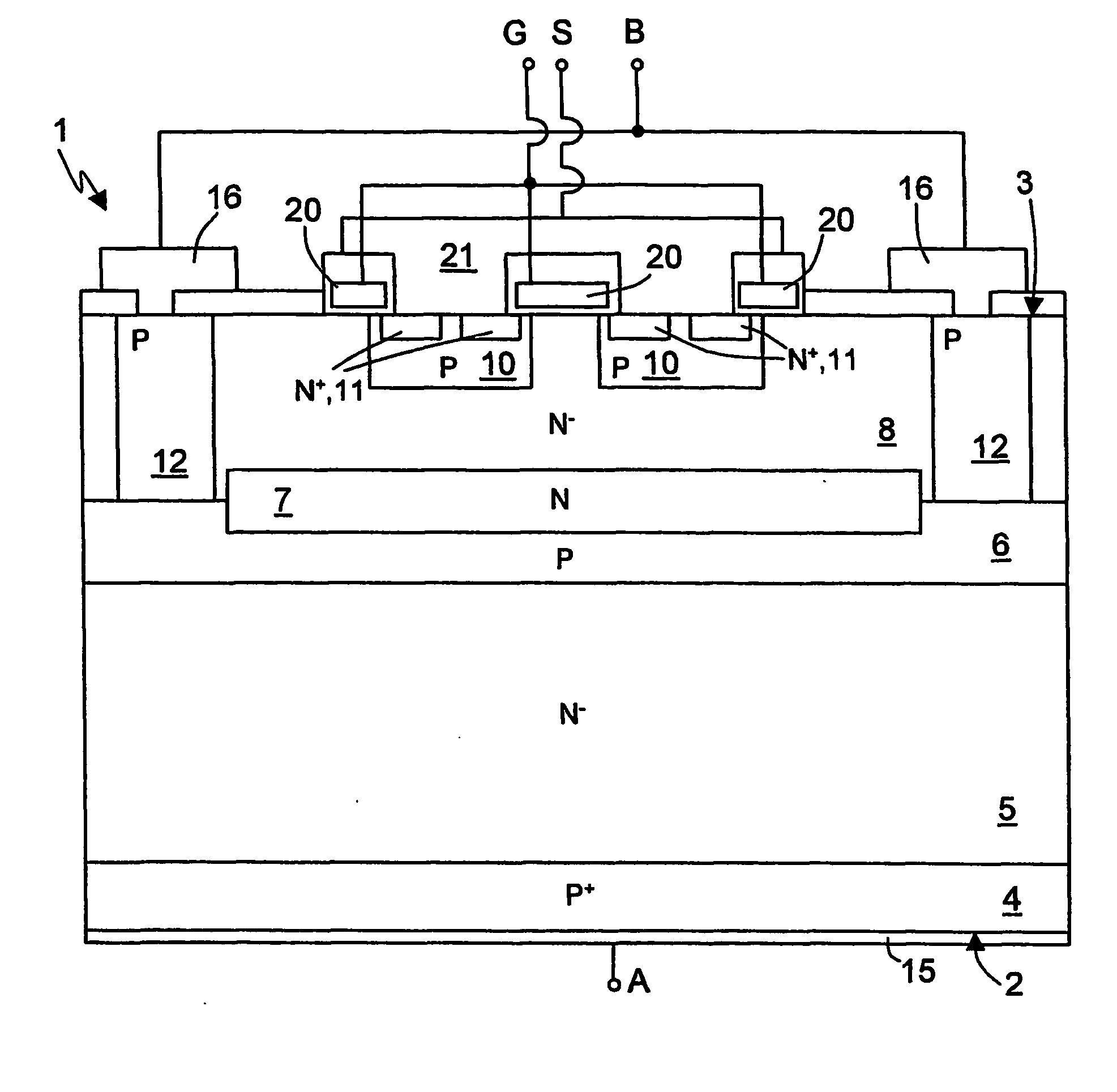
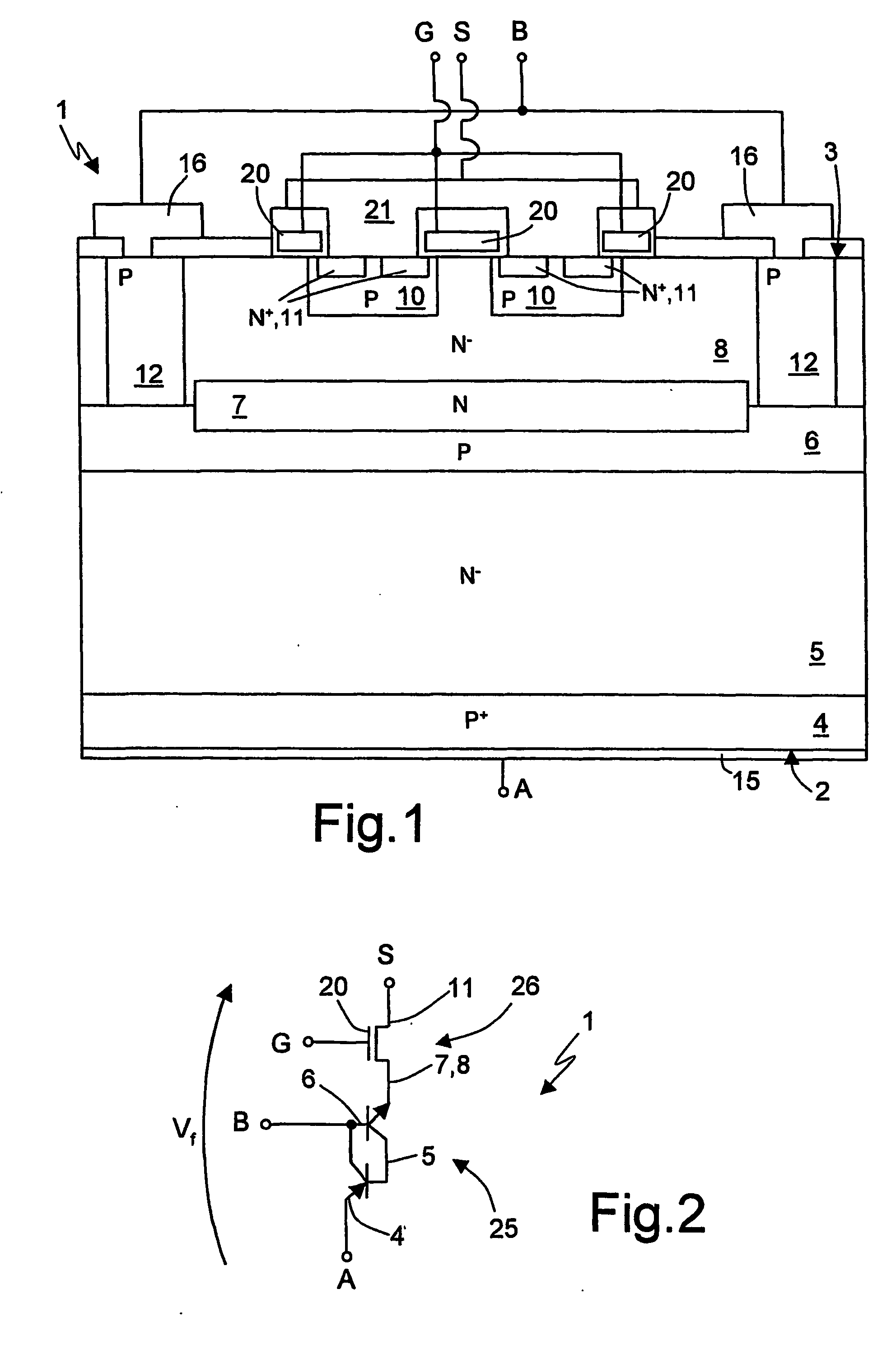
[0015]FIG. 1 is a cross-section of an elementary structure of a power device 1 according to one embodiment of the invention. The power device 1 may in any case comprise a plurality of elementary structures arranged alongside one another. Each elementary structure may moreover comprise one or more MOSFET cells. In the embodiment illustrated in FIG. 1, the elementary structure comprises two elementary cells.

[0016] According to FIG. 1. (not drawn to scale in the vertical direction), the power device 1 is formed by a body of semiconductor material, which has a bottom surface 2 and a top surface 3 and comprises: a substrate 4 of P+-type; a first base region, also referred hereinafter as drift region 5, of N−-type; a second base region, referred hereinafter as base region 6, of P-type; a cathode region 7, of N-type; and an epitaxial region 8, of N−-type. The epitaxial region 8 moreover accommodates body regions 10, source regions 11, and a deep well 12.

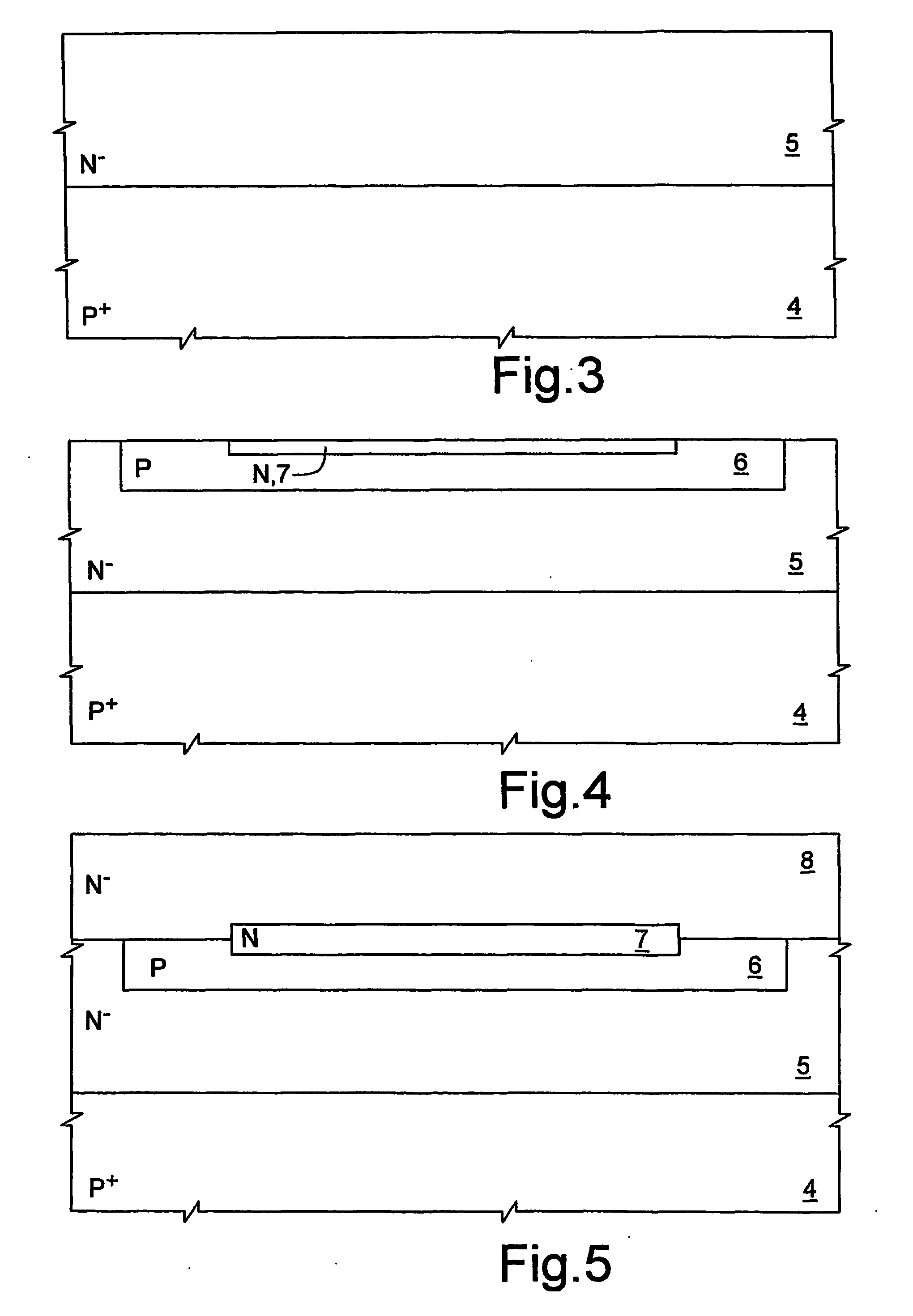
[0017] The bottom surface 2 of the...


PUM


Abstract

A power device is formed by a thyristor and by a MOSFET transistors, series-connected between a first and a second current-conduction terminal. The power device moreover has a control terminal connected to an insulated-gate electrode of the MOSFET transistor and receiving a control voltage for turning on/off the device, and a third current-conduction terminal connected to the thyristor for fast extraction of charges during turning-off. Thereby, upon turning off, there are no current tails, and turning off is very fast. The power device does not have parasitic components and consequently has a very high reverse-bias safe-operating area.

Description

TECHNICAL FIELD [0001] The present invention relates in general to the field of power devices, and more in particular to a power device usable as a power actuator. BACKGROUND ART [0002] As is known, power actuators must keep down to a minimum the dissipation of power both when on and during switching. [0003] For this reason, for implementing a power actuator, there has been a passage from bipolar transistors (which have low on-dissipation) and from MOS transistors, (which have low dissipation during switching) to hybrid components that combine the advantages of both types. [0004] In addition, power actuators must also have high input impedance and hence be driven with low-voltage pulses. Consequently, the various hybrid solutions that have been proposed (such as, insulated-gate bipolar transistors—IGBTs, MOS-controlled thyristors—MCTs, and emitter-switched thyristors—ESTs), in addition to presenting different levels of compromise between power dissipation when on and during switchin...

Claims


Application Information

Patent Timeline
IPC IPC(8): H01L29/76H01L21/332H01L29/745
CPCH01L29/66378H01L29/7455
Inventor RONSISVALLE, CESARE
Owner STMICROELECTRONICS SRL
Why Eureka
Try Eureka