Bidirectional mos device and method for preparing the same

a metaloxidesemiconductor and bidirectional technology, applied in the direction of semiconductor devices, transistors, electrical devices, etc., can solve the problems of transverse or longitudinal breakdown, reduce the performance of mos devices, conventional bidirectional mos devices have a large size and large drift region resistance, etc., to reduce the drift region resistance, high breakdown voltage, low voltage

Inactive Publication Date: 2017-03-23
UNIV OF ELECTRONICS SCI & TECH OF CHINA +1
View PDF7 Cites 2 Cited by
  • Summary
  • Abstract
  • Description
  • Claims
  • Application Information

AI Technical Summary

Benefits of technology

[0038]A U-shaped symmetrical drift region, comprising the dielectric slot, the N-type region, the first filling slot, the second filling slot, (the first filling slot and the second filling slot are symmetrically arranged), the first N-type layer, the second N-type layer, (the first N-type layer and the second N-type layer are symmetrically arranged), the first P-type region, and the second P-type region (the first P-type region and the second P-type region are symmetrically arranged) is able to achieve a high breakdown voltage and a low voltage drop or on-resistance at a certain width of the device. Thus the bidirectional MOS device is a symmetrical field stop device. At the IGBT work mode, the MOS device is an IGBT device featuring carrier storage layer and field stop layer; at the MOS work mode, the bidirectional MOS device is an MOS device featuring highly doped layer operating to decrease the resistance of the drift region and field stop layer. The compound effect of the U-shaped drift region prevents the transverse and longitudinal breakdown of the device, and endows the device with favorable voltage endurance per unit drift region length and low voltage drop and on-resistance, thereby obviously improving the performance of the device.

Problems solved by technology

However, the blockage of any one of the devices tends to result in transverse or longitudinal breakdown.
Thus, the conventional bidirectional MOS devices have big size and large resistance of the drift region.
This reduces the performance of the MOS devices.

Method used


Image

  • Bidirectional mos device and method for preparing the same
  • Bidirectional mos device and method for preparing the same
  • Bidirectional mos device and method for preparing the same

Examples


example 1

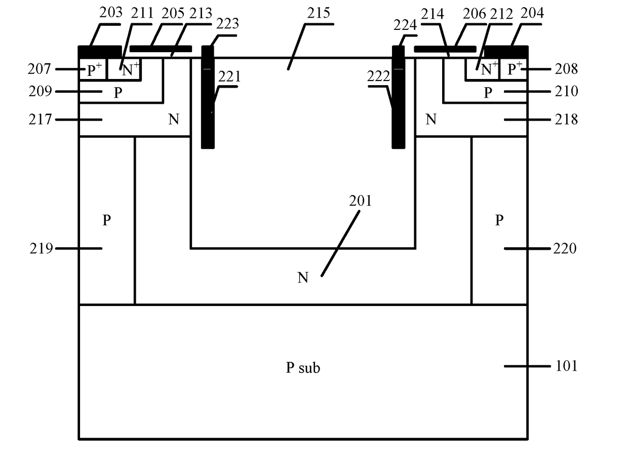
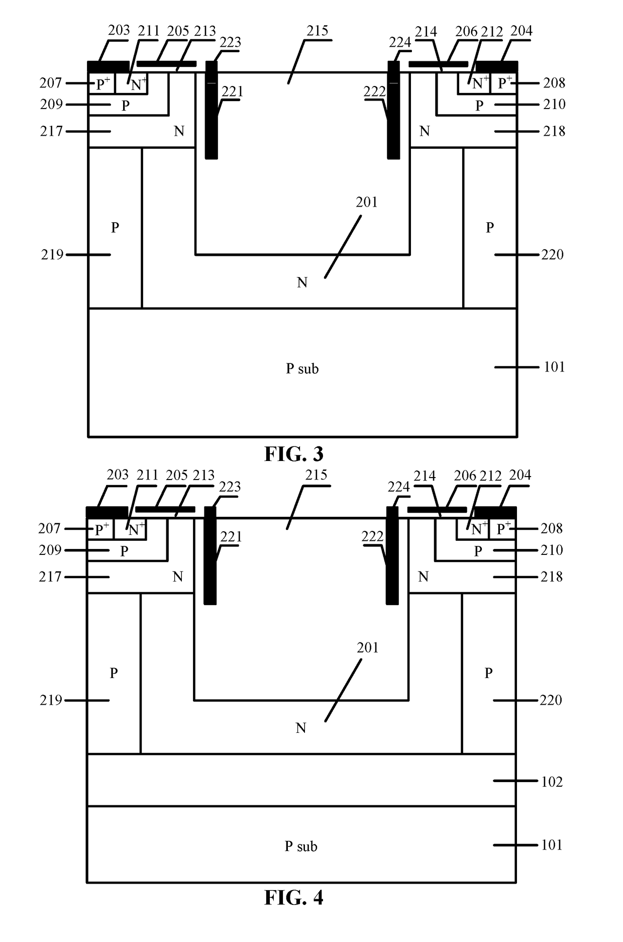
[0059]FIG. 3 is schematic diagram of a cell structure of a bidirectional MOS device. As shown in FIG. 3, the bidirectional MOS device comprises a P-type substrate 101 and an active region. The active region is disposed on an upper surface of the P-type substrate 101. The active region comprises a drift region, a first MOS structure and a second MOS structure. The first MOS structure and the second MOS structure are symmetrically disposed on two ends of an upper layer of the drift region.

[0060]The first MOS structure comprises a first P-type body region 209, a first P+ contact region 207, a first N+ source region 211, a first metal electrode 203, and a first gate structure. The first P+ contact region 207 and the first N+ source region 211 are disposed in the first P-type body region 209. The first metal electrode 203 and the first gate structure are disposed on an upper surface of the first P-type body region 209. The first P+ contact region 207 and the first N+ source region 211 ar...

example 2

[0072]As shown in FIG. 4, the device in the example follows a basic structure in Example 1, except that a dielectric buried layer 102 is disposed between the P-type substrate 101 and the N-type region 201, the first P-type region 219, and the second P-type region 220.

[0073]The device in the example follows a basic working principle in Example 1, except that the dielectric buried layer is adapted to isolate the P-type substrate 101 from the active region, and the leakage current of the P-type substrate is modified; especially at the IGBT work mode, when the device is turned on, the MOS device as the collector having the high potential injects current to the electron holes of the P-type substrate, thus reducing the loss of the device, and isolating the MOS device from other devices.

example 3

[0074]As shown in FIG. 5, the device in the example follows a basic structure in Example 1, except that a third P-type region 225 is disposed between a lower part of the dielectric slot 215 and the N-type region 201.

[0075]The device in the example follows a basic working principle in Example 1, except that the third P-type region 225 is adapted to provide an additional charge depletion effect when the device is blocked, thus the breakdown voltage of the device and the doping concentration of N-type region 201 can be further improved, and the performance of the device is further enhanced.


PUM


Abstract

A bidirectional Metal-Oxide-Semiconductor (MOS) device, including a P-type substrate, and an active region. The active region includes a drift region, a first MOS structure and a second MOS structure; the first MOS structure includes a first P-type body region, a first P+ contact region, a first N+ source region, a first metal electrode, and a first gate structure; the second MOS structure includes a second P-type body region, a second P+ contact region, a second N+ source region, a second metal electrode, and a second gate structure; and the drift region includes a dielectric slot, a first N-type layer, a second N-type layer, and an N-type region. The active region is disposed on the upper surface of the P-type substrate. The first MOS structure and the second MOS structure are symmetrically disposed on two ends of the upper layer of the drift region.

Description

CROSS-REFERENCE TO RELATED APPLICATIONS[0001]This application is a continuation-in-part of International Patent Application No. PCT / CN2014 / 094626 with an international filing date of Dec. 23, 2014, designating the United States, now pending, the contents of which, including any intervening amendments thereto, are incorporated herein by reference. Inquiries from the public to applicants or assignees concerning this document or the related applications should be directed to: Matthias Scholl P. C., Attn.: Dr. Matthias Scholl Esq., 245 First Street, 18th Floor, and Cambridge, Mass. 02142.BACKGROUND OF THE INVENTION[0002]Field of the Invention[0003]The invention relates to a bidirectional Metal-Oxide-Semiconductor (MOS) device and a method for preparing the same.[0004]Description of the Related Art[0005]As shown in FIGS. 1-2, conventional bidirectional MOS devices share one drift region (N-type well) to reduce the length of the drift region. However, the blockage of any one of the device...

Claims


Application Information

Patent Timeline
Patent Type & Authority Applications(United States)
IPC IPC(8): H01L29/74H01L29/10H01L21/02H01L29/66H01L21/3065H01L21/265H01L29/747H01L29/40
CPCH01L29/7424H01L29/747H01L29/1095H01L21/02233H01L29/66386H01L21/3065H01L21/26586H01L29/408H01L29/407H01L29/7394H01L29/0623H01L29/7398H01L29/0649H01L29/7809H01L29/7812H01L29/0634H01L29/66333H01L29/66712H01L29/7831H01L29/78H01L29/66325H01L29/7395
Inventor ZHANG, JINPINGLI, ZEHONGLIU, JINGXIUREN, MINZHANG, BOLI, ZHAOJI
Owner UNIV OF ELECTRONICS SCI & TECH OF CHINA
Why Eureka
Try Eureka