Differential Source Follower having 6dB Gain with Applications to WiGig Baseband Filters

a technology of baseband filter and differential source follower, which is applied in the direction of pulse manipulation, pulse technique, instruments, etc., can solve the problems of much more difficult design of high-performance systems in low-power supply integrated circuits, and achieve high input impedance, good current drive, and extended high frequency behavior of filters

US20130076434A1Active Publication Date: 2013-03-28TENSORCOM
0 Cites 15 Cited by

Patent Information

Authority / Receiving Office
US · United States
Patent Type
Applications(United States)
Current Assignee / Owner
Publication Date
2013-03-28

Smart Images

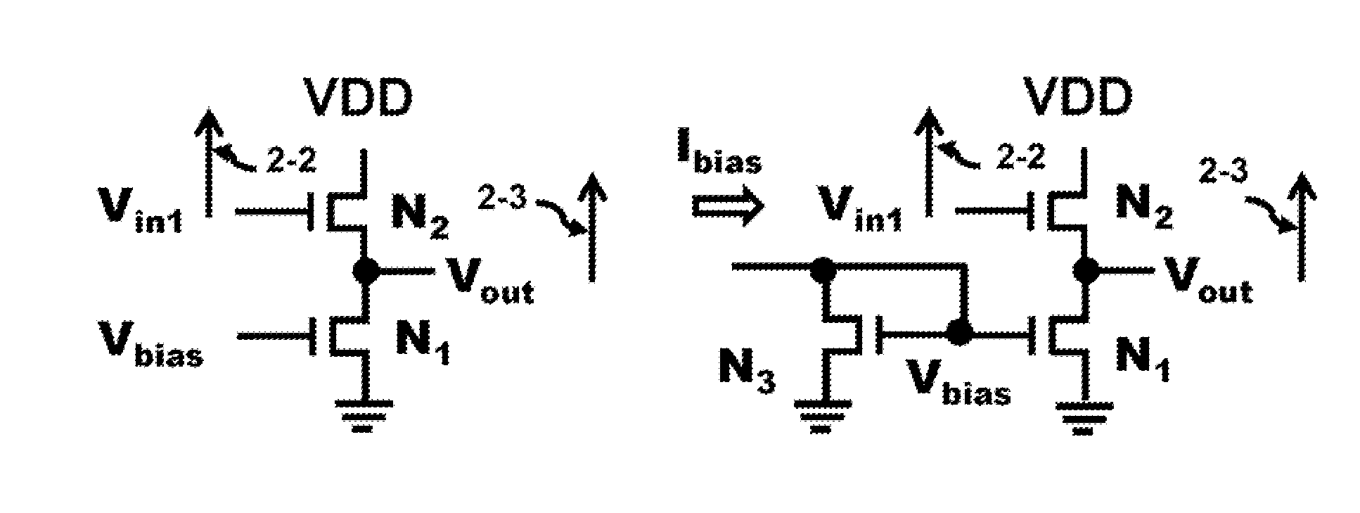
  • Figure 1
    Figure 1
  • Figure 2
    Figure 2
  • Figure 3
    Figure 3
Patent Text Reader

Abstract

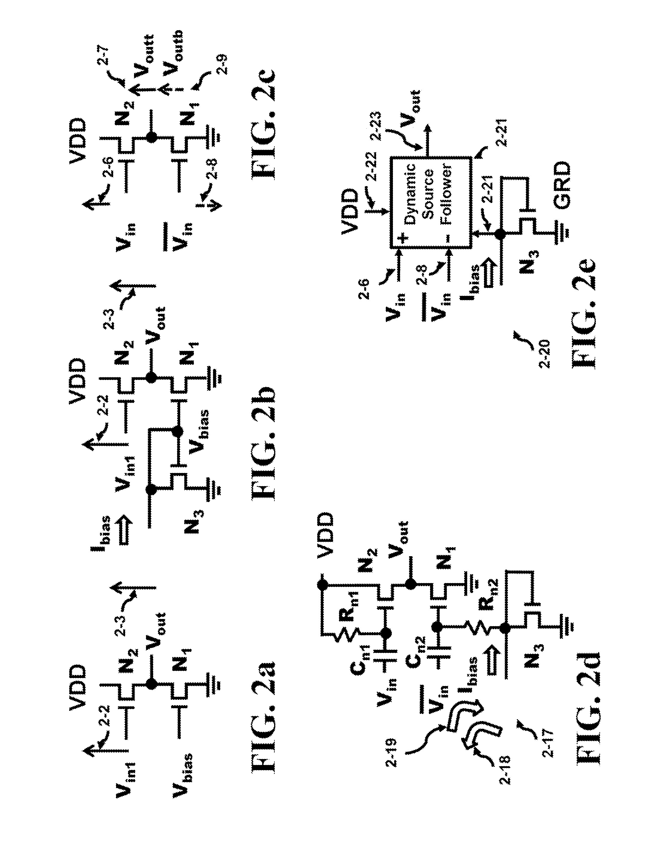
A Sallen-Key filter requires an operational amplifier with a large input impedance and a small output impedance to meet the external filter characteristics. The operational amplifier requires an internal feedback path for stability that limits performance. This invention eliminates the need for internal feedback and increases the gain of a source follower which has characteristics matching the operational amplifier in the Sallen-Key filter. The source follower provides 6 dB of AC voltage gain and is substituted for the operational amplifier in the Sallen-Key filter. The Sallen-Key filter requires a differential configuration to generate all the required signals with their compliments and uses these signals in a feed forward path. Furthermore, since the source follower uses only two n-channel stacked devices, the headroom voltage is maximized to several hundred millivolts for a 1.2V voltage supply in a 40 nm CMOS technology. Thus, the required 880 MHz bandwidth of the Sallen-Key filter can be easily met using the innovative source follower.
Need to check novelty before this filing date? Find Prior Art

Description

CROSS REFERENCE TO RELATED APPLICATIONS

[0001] The present application is related to the co-filed U.S. application entitled “A High Performance Divider Using Feed Forward, Clock Amplification and Series Peaking Inductors”, and the co-filed U.S. application entitled “Method and Apparatus of Minimizing Extrinsic Parasitic Resistance in 60 GHz Power Amplifier Circuit? both filed on Sep. 23, 2011, which are invented by the same inventor as the present application and incorporated herein by reference in their entireties.BACKGROUND OF THE INVENTION

[0002] The Federal Communications Commission (FCC) has allotted a spectrum of bandwidth in the 60 GHz frequency range (57 to 64 GHz). The Wireless Gigabit Alliance (WiGig) is targeting the standardization of this frequency band that will support data transmission rates up to 7 Gbps. Integrated circuits, formed in semiconductor die, offer high frequency operation in this millimeter wavelength range of frequencies. Some of these integrated circuits u...

Examples

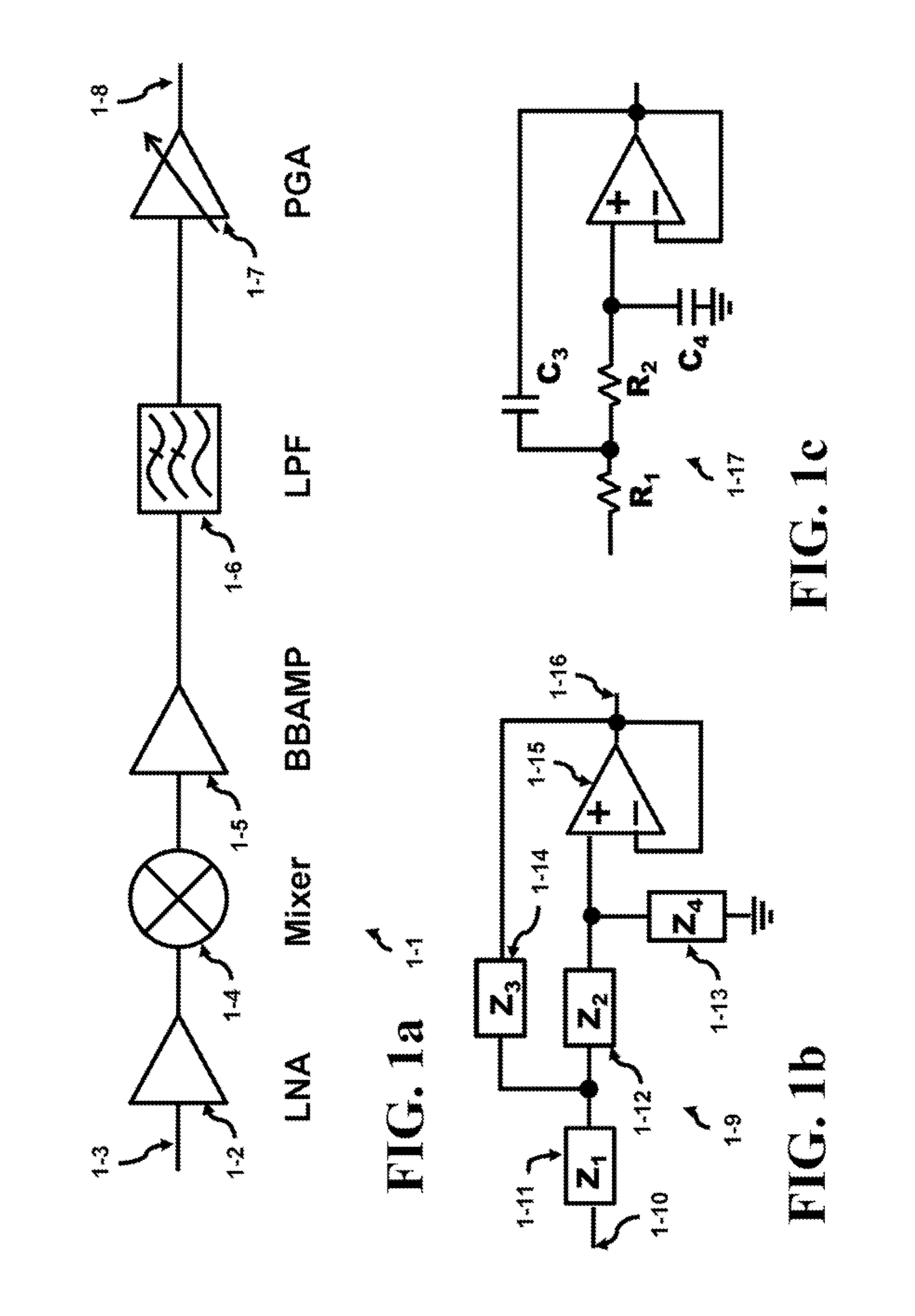
Embodiment Construction

[0035]The inventions presented in this specification can be used in any wired or wireless high frequency system design. One application of the inventions can be applied to the front end of a receiver circuit 1-1 as illustrated in FIG. 1a. The Low Noise Amplifier (LNA) 1-2 can receive a weak signal at its input 1-3. This signal may have been be provided by an antenna or a wired line and is amplified by the LNA and applied to the Mixer 1-4. The CMOS design of an LNA at millimeter waves with a gain greater than 30 dB is very difficult. Afterwards, the signal is demodulated into a baseband signal. The baseband signal is amplified by the Base Band Amplifier (BBAMP) 1-5 and sent to the Low Pass Filter (LPF) 1-6. The LPF filters the signal and also provides an additional gain before the signal is sent to the Programmable Gain Amplifier (PGA) 1-7 which generates an output 1-8. In either case, the weak signal is amplified, demodulated, amplified, filtered and amplified as an output 1-8 befor...