Integrated circuit inductors

a technology of integrated circuits and inductors, applied in the field of inductors, can solve the problems of poor q value of inductors, low efficiency of inductors, degrade circuit performance, etc., and achieve the effect of improving the q-factor of inductors

Inactive Publication Date: 2006-11-14
ALTERA CORP
View PDF15 Cites 50 Cited by
  • Summary
  • Abstract
  • Description
  • Claims
  • Application Information

AI Technical Summary

Benefits of technology

[0011]An integrated circuit inductor may be based on a conductive inductor line that forms a spiral on the surface of the integrated circuit. The Q-factor of the integrated circuit may be enhanced by reducing the resistance of the conductive inductor line and by reducing undesirable power losses due to electromagnetic interactions between the inductor and the underlying semiconductor substrate of the integrated circuit.
[0022]Using these arrangements, the Q-factor of the inductor may be improved without disrupting the normal process steps used during fabrication of the integrated circuit. For example, these arrangements may be used to form high-quality-factor inductors without the use of extensive post-processing steps to build up the inductor conductors or the use of feature sizes that would violate the normal design rules of the semiconductor fabrication process.

Problems solved by technology

Inductors with low Q values are inefficient and can degrade circuit performance.
Conductors with relatively higher resistance produce inductors with poor Q values.
However, tungsten is not highly conductive and the connections between the upper-layer aluminum line and lower-layer aluminum line are only made at a finite number of locations, so the resistance of the inductor lines formed in this way can still be higher than desired.
However, many integrated circuit processes do not allow thick metal lines to be formed.
Although lines can sometimes be thickened using special post-processing procedures, the resulting increase in process complexity can have an adverse impact on cost and reliability.
Moreover, regardless of the process that is used, the line width cannot be too large, because this can lead to capacitive coupling with the silicon substrate, which reduces Q.

Method used


Image

  • Integrated circuit inductors
  • Integrated circuit inductors
  • Integrated circuit inductors

Examples


Embodiment Construction

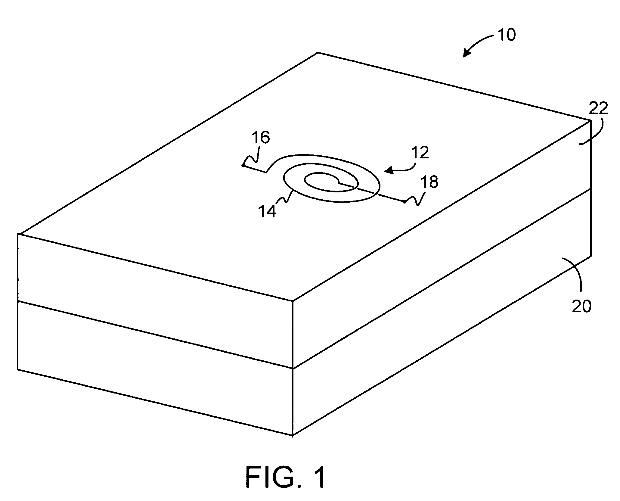
[0048]An illustrative integrated circuit 10 having an integral integrated circuit inductor 12 is shown in FIG. 1. Inductor 12 is formed by coiling a conductive line 14 so that magnetic flux is channeled through its center. During operation of inductor 12, alternating current (AC) signals are applied to conductive inductor line 14 using terminal 16 and terminal 18.

[0049]The integrated circuit 10 may be formed from a semiconductor substrate 20 in which transistors and other semiconductor devices are formed. During operation of integrated circuit 10, these devices interact with inductor 12 through conductive lines connected to terminal 16 and terminal 18. Because inductor 12 is formed on the same integrated circuit structure as the transistors and other devices, it is not necessary to connect inductor 12 to the circuitry of circuit 10 through a special package or external wires. This can improve the performance of circuit 10, while reducing cost and increasing reliability.
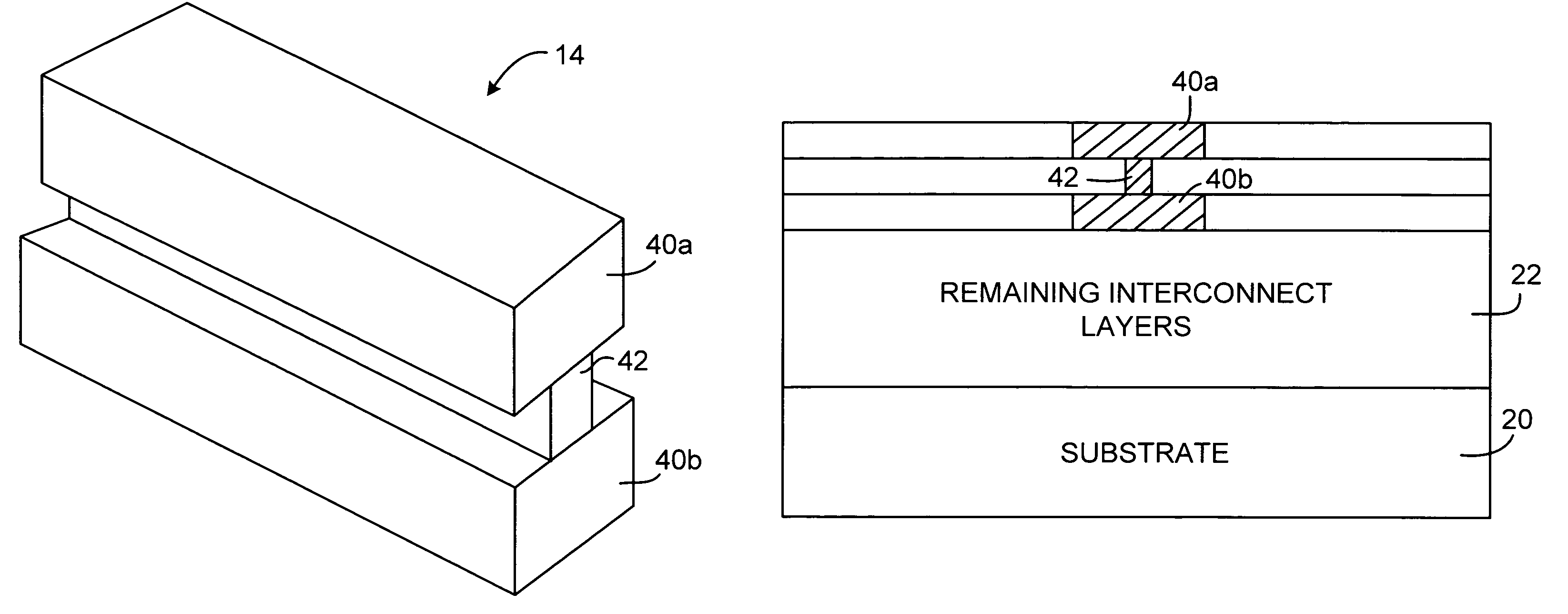
[0050]The sub...


PUM

PropertyMeasurementUnit
depthsaaaaaaaaaa
widthaaaaaaaaaa
sizeaaaaaaaaaa

Abstract

Integrated circuit inductors may be formed using a spiral layout on the surface of an interconnect dielectric stack. Conductive lines from two or more metal layers in the interconnect stack may be electrically connected using one or more via trenches. The via trench interconnection arrangement reduces the resistance of the inductor and increases the inductor's Q-factor. The Q-factor of the inductor may also be increased by placing a region of n-type and p-type wells or a metal plate region beneath the inductor to reduce power losses during operation. Shallow trench isolation may be used to reduce eddy currents and increase Q. The effects of copper dishing and trench blow-out may be used during inductor fabrication. A dual damascene fabrication process may be used.

Description

BACKGROUND OF THE INVENTION[0001]This invention relates to inductors, and more particularly, to inductors formed on integrated circuits.[0002]Integrated circuits are used in a variety of electronic equipment. It is often necessary to use inductors with such circuits. For example, the circuitry used for radio-frequency (RF) applications, microwave applications, and many analog circuit applications can require inductors.[0003]Although it is sometimes possible to make use of discrete inductors, inductors that are formed on the integrated circuit itself are often preferred or required for performance and economic reasons. Fabricating an inductor as part of an integrated circuit structure eliminates the need for special packaging and can enhance reliability. Integrated circuit inductors are typically spiral in shape and are formed on the top surface of the circuit.[0004]An important figure of merit for an integrated circuit inductor is its quality factor Q. The quality factor Q for an in...

Claims


Application Information

Patent Timeline
Patent Type & Authority Patents(United States)
IPC IPC(8): H01F5/00H01F7/06
CPCH01F17/0013H01F41/041H01L21/761H01L23/5227H01L27/08H01F27/34Y10T29/4902H01F27/362H01F27/40H01F2017/002H01F2017/0053H01L2924/0002Y10T29/49071H01L2924/00H01F27/36H01F27/363
Inventor SIDHU, LAKHBEER S.RAHIM, IRFAN
Owner ALTERA CORP
Why Eureka
Try Eureka