High Q factor integrated circuit inductor

a high-quality, inductor technology, applied in the direction of transformer/inductance coil/winding/connection, transformer/inductance magnetic core, inductance, etc., can solve the problems of large integrated circuit chip surface area of metal lines inductors, power consumption increase, and inability to meet the requirements of high-quality inductors,

Active Publication Date: 2005-08-04
GLOBALFOUNDRIES US INC
View PDF22 Cites 50 Cited by
  • Summary
  • Abstract
  • Description
  • Claims
  • Application Information

AI Technical Summary

Problems solved by technology

As the RF frequency that integrated circuits operate at increases, power consumption increases unless the Q factor of the inductors increase as well.
However, the use of wide metal lines inductors can consume large amounts of integrated circuit chip surface and suitable areas of an integrated

Method used


Image

  • High Q factor integrated circuit inductor
  • High Q factor integrated circuit inductor
  • High Q factor integrated circuit inductor

Examples


first embodiment

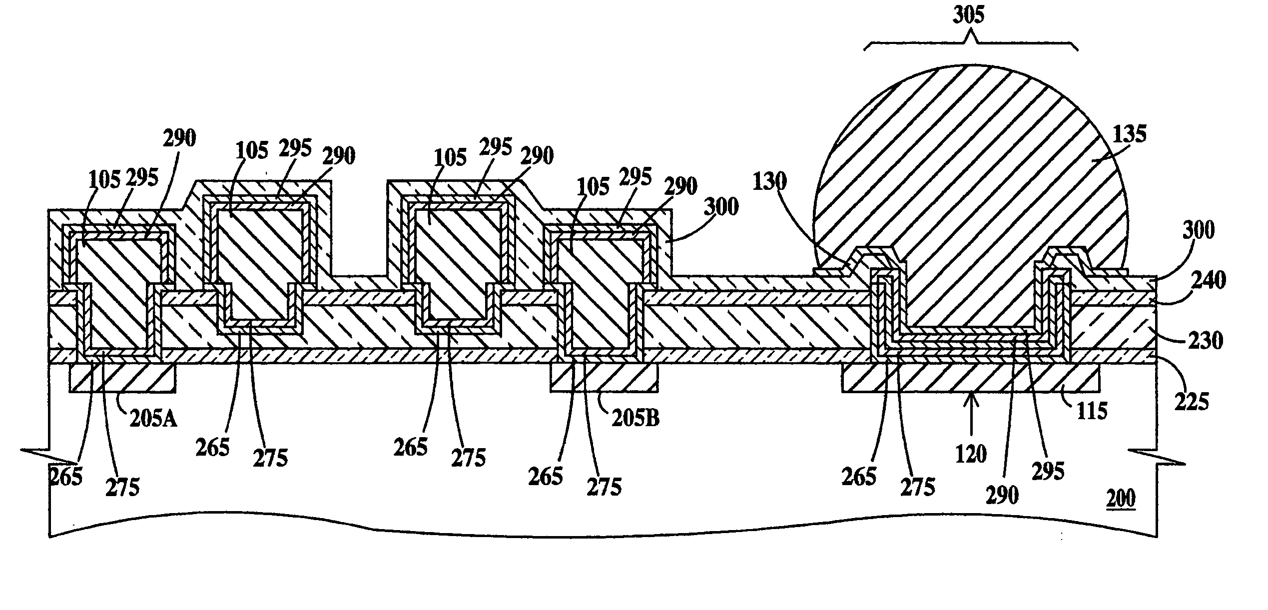
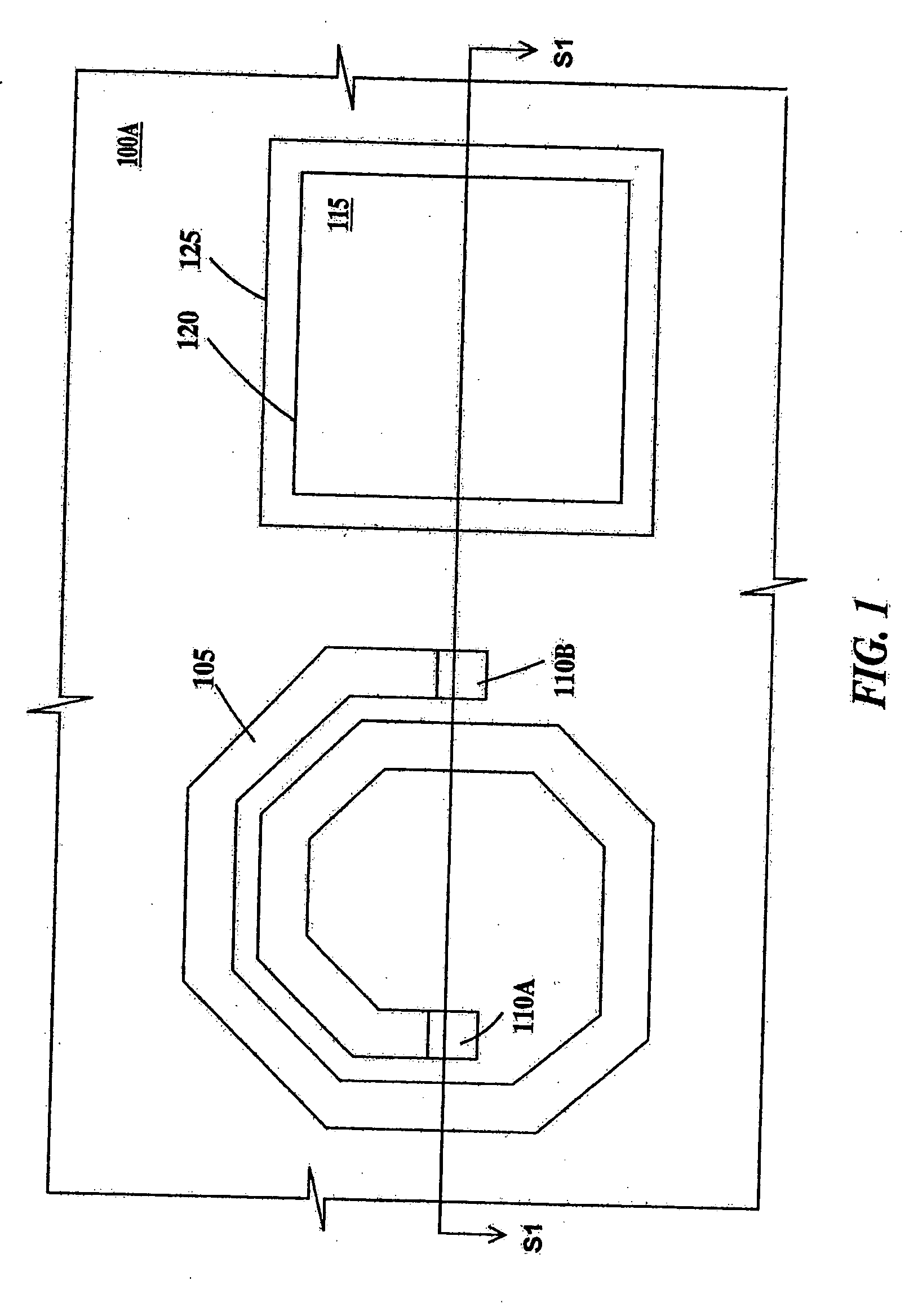
[0015]FIG. 1 is a top view of an inductor and contact pad according is according to the present invention. In FIG. 1, an integrated circuit chip 100A includes an inductor 105 having integral vias 110A and 110B for interconnection to wiring levels (not shown) within the integrated circuit chip. While inductor 105 is illustrated as a spiral inductor the invention is applicable to inductors of other shapes as well. Integrated circuit chip 100A also includes an I / O terminal pad 115 in the bottom of a via 120 for interconnection to wiring levels (not shown) within the integrated circuit chip and a conductive passivation layer 125 formed on top of I / O terminal pad 115 and overlapping via 120.

second embodiment

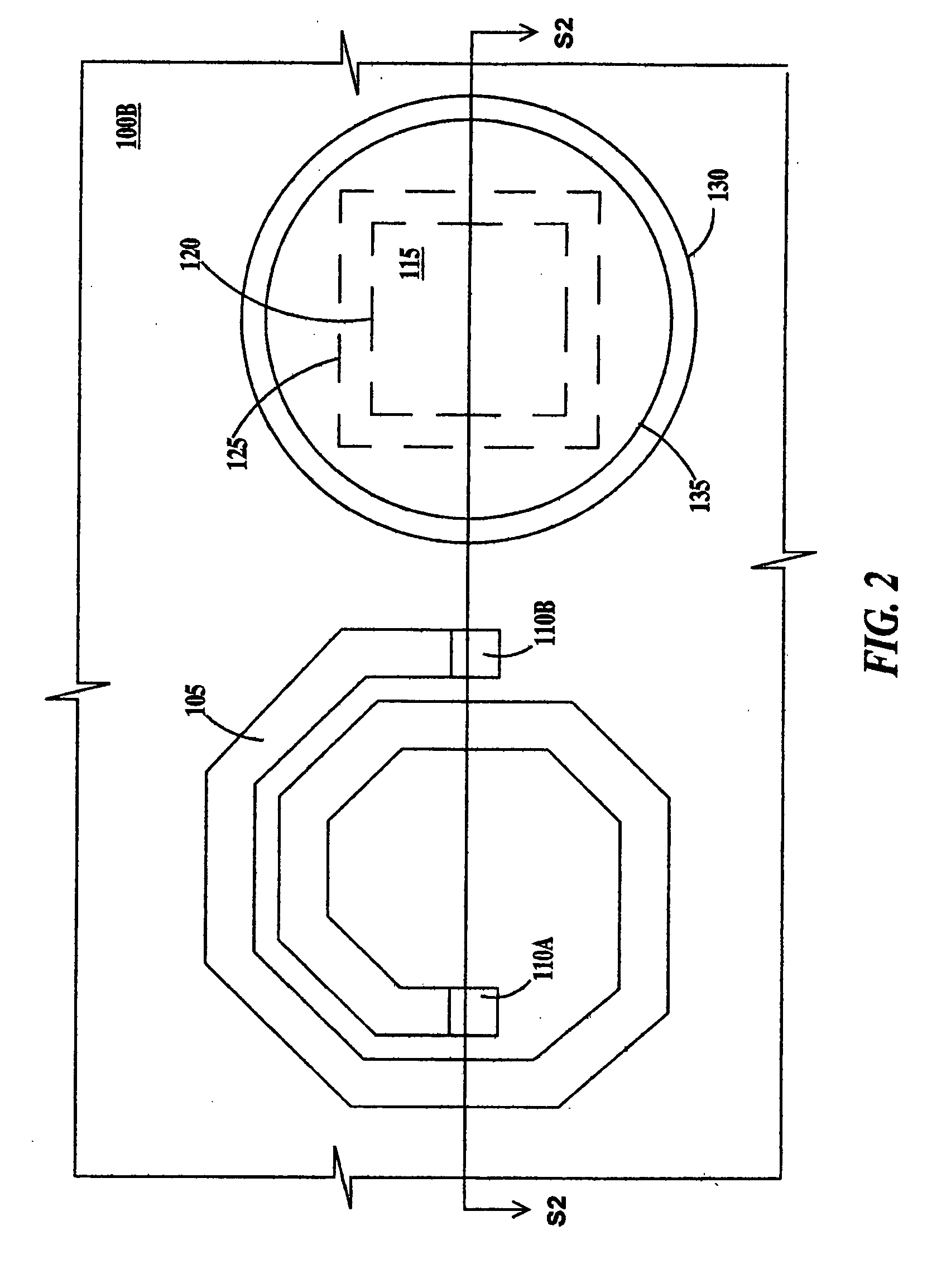
[0016]FIG. 2 is a top view of an inductor and contact pad according is according to the present invention. In FIG. 2, an integrated circuit chip 100B includes inductor 105 having integral vias 110A and 110B for interconnection to wiring levels (not shown) within the integrated circuit chip. While inductor 105 is illustrated as a spiral inductor the invention is applicable to inductors of other shapes as well. Integrated circuit chip 100B also includes I / O terminal pad 115 in the bottom of via 120 for interconnection to wiring levels (not shown) within the integrated circuit chip, conductive passivation layer 125 formed on top of I / O terminal pad 115 and overlapping via 120, a pad limiting metallurgy (PLM) layer 130 and a solder ball 135 formed over conductive passivation layer 125. Solder balls are also known as controlled collapse chip connection (C4) balls, C4 solder balls and solder bumps. For the purposes of the present invention the term solder ball may be replaced with the ter...

third embodiment

[0017]FIG. 3 is a top view of an inductor and contact pad according is according to the present invention. In FIG. 3, an integrated circuit chip 100C includes inductor 105 having integral vias 110A and 110B for interconnection to wiring levels (not shown) within the integrated circuit chip. While inductor 105 is illustrated as a spiral inductor the invention is applicable to inductors of other shapes as well. Integrated circuit chip 100C also includes I / O terminal pad 115 in the bottom of via 120 for interconnection to wiring levels (not shown) within the integrated circuit chip, a conductive passivation coated raised pad 140 formed on top and overlapping via 120, PLM layer 130 and solder ball 135 formed over conductive passivation layer 125. PLM layer 130 is fully landed on raised pad 140.

[0018]FIGS. 4A through 4F are partial cross-sectional views illustrating fabrication steps common to the first, second and third embodiments of the present invention. FIGS. 4A through 4F may be ta...


PUM


Abstract

An inductor and a method of forming and the inductor, the method including: (a) providing a semiconductor substrate; (b) forming a dielectric layer on a top surface of the substrate; (c) forming a lower trench in the dielectric layer; (d) forming a resist layer on a top surface of the dielectric layer; (e) forming an upper trench in the resist layer, the upper trench aligned to the lower trench, a bottom of the upper trench open to the lower trench; and (f) completely filling the lower trench at least partially filling the upper trench with a conductor in order to form the inductor. The inductor including a top surface, a bottom surface and sidewalls, a lower portion of said inductor extending a fixed distance into a dielectric layer formed on a semiconductor substrate and an upper portion extending above said dielectric layer; and means to electrically contact said inductor.

Description

FIELD OF THE INVENTION [0001] The present invention relates to the field of integrated circuits; more specifically, it relates to high quality (Q) factor inductor structures, methods of fabricating high Q factor inductor structures and methods of integration of high Q factor inductor structures into integrated circuit manufacturing processes. BACKGROUND OF THE INVENTION [0002] Inductors are used in many integrated circuits intended for radio-frequency (RF) applications. Inductors are typically fabricated of relatively thick metals on or near the surface of integrated circuit chips. As the RF frequency that integrated circuits operate at increases, power consumption increases unless the Q factor of the inductors increase as well. The Q factor of an inductor is defined as Q=Es / El, where Es is the amount energy that is stored in the reactive portion of the inductor and El is the amount of energy that is lost in the reactive portion of the inductor. The Q value of an inductor can also b...

Claims


Application Information

Patent Timeline
IPC IPC(8): H01F41/04H01F17/00H01L21/02H01L23/485H01L23/522H01L23/532H01L27/08
CPCH01L23/5227H01L23/53238H01L24/03H01L24/05H01L24/12H01L27/08H01L28/10H01L2224/0401H01L2224/05022H01L2224/05084H01L2224/05557H01L2224/05624H01L2224/05644H01L2224/13007H01L2224/13022H01L2224/13023H01L2224/13099H01L2924/01002H01L2924/01004H01L2924/01005H01L2924/01006H01L2924/01013H01L2924/01014H01L2924/01022H01L2924/01027H01L2924/01028H01L2924/01029H01L2924/01033H01L2924/01042H01L2924/0105H01L2924/01073H01L2924/01074H01L2924/01078H01L2924/01079H01L2924/01082H01L2924/014H01L2924/04953H01L2924/05042H01L2924/14H01L2924/19042H01L2924/30107H01L2924/01019H01L2924/01024H01L2924/01072H01L2224/48624H01L2224/48644H01L2224/45144H01L2224/05027H01L2224/05014H01L2224/0508H01L2224/05555H01L2224/05558H01L2224/05007H01L2224/45124H01L2224/04042H01L2924/00014H01L2924/00H01L2224/48724H01L2224/48744
Inventor EDELSTEIN, DANIEL C.ANDRICACOS, PANAYOTIS C.COTTE, JOHN M.DELIGIANNI, HARIKLIAMAGERLEIN, JOHN H.PETRARCA, KEVIN S.STEIN, KENNETH J.VOLANT, RICHARD P.
Owner GLOBALFOUNDRIES US INC
Why Eureka
Try Eureka