Detect developed bad blocks in non-volatile memory devices

a non-volatile memory and block technology, applied in cleaning equipment, lighting and heating equipment, instruments, etc., can solve the problems of poor block development, block physical defects which can become worse, and few bad blocks may be developed during us

Active Publication Date: 2017-10-12
SK HYNIX INC
View PDF1 Cites 31 Cited by
  • Summary
  • Abstract
  • Description
  • Claims
  • Application Information

AI Technical Summary

Benefits of technology

[0008]Embodiments of the invention pertain to systems, methods, and computer-readable instructions to provide an improved Background media scan (BGMS) process to detect a developed bad block during the flash memory usage. At the end of a block read, if it is determined that a maximum error rate of a word-line is significant higher than a corresponding average error rate (above a pre-determined ratio), the improved BGMS process can predict that the word-line with the maximum error rate is likely to develop into a bad word-line. Further if this maximum error rate is above a pre-determined threshold, the block can be retired.

Problems solved by technology

NAND flash devices are not always manufactured perfectly.
For example, some blocks may have physical defects which can become worse with time.
In some instances, a few bad blocks may be developed during usage.
The bad blocks developed during usage are called developed bad blocks and may fail much earlier than normal blocks.
Bad blocks can develop erratically and may be hard to predict.
For example, in some instances, elevated heat or multiple program-erase (P / E) cycles can make the NAND flash devices susceptible to bit errors, thus causing them likely to fail.
However, in some instances, not all errors can be corrected.
ChipKill can be a costly feature in flash devices as it can affect size of system data area, cost of development (hardware / firmware), Application Specific Integrated Circuit (ASIC) layout real estate, and power.
Data have shown that most of the catastrophic failures taking place in the developed bad blocks are localized on a single or two neighboring word-lines (WLs), and they are caused by gradually developed defects.
However, such an approach cannot detect the sign of a developed bad block and / or predict its failure.

Method used


Image

  • Detect developed bad blocks in non-volatile memory devices
  • Detect developed bad blocks in non-volatile memory devices
  • Detect developed bad blocks in non-volatile memory devices

Examples


Embodiment Construction

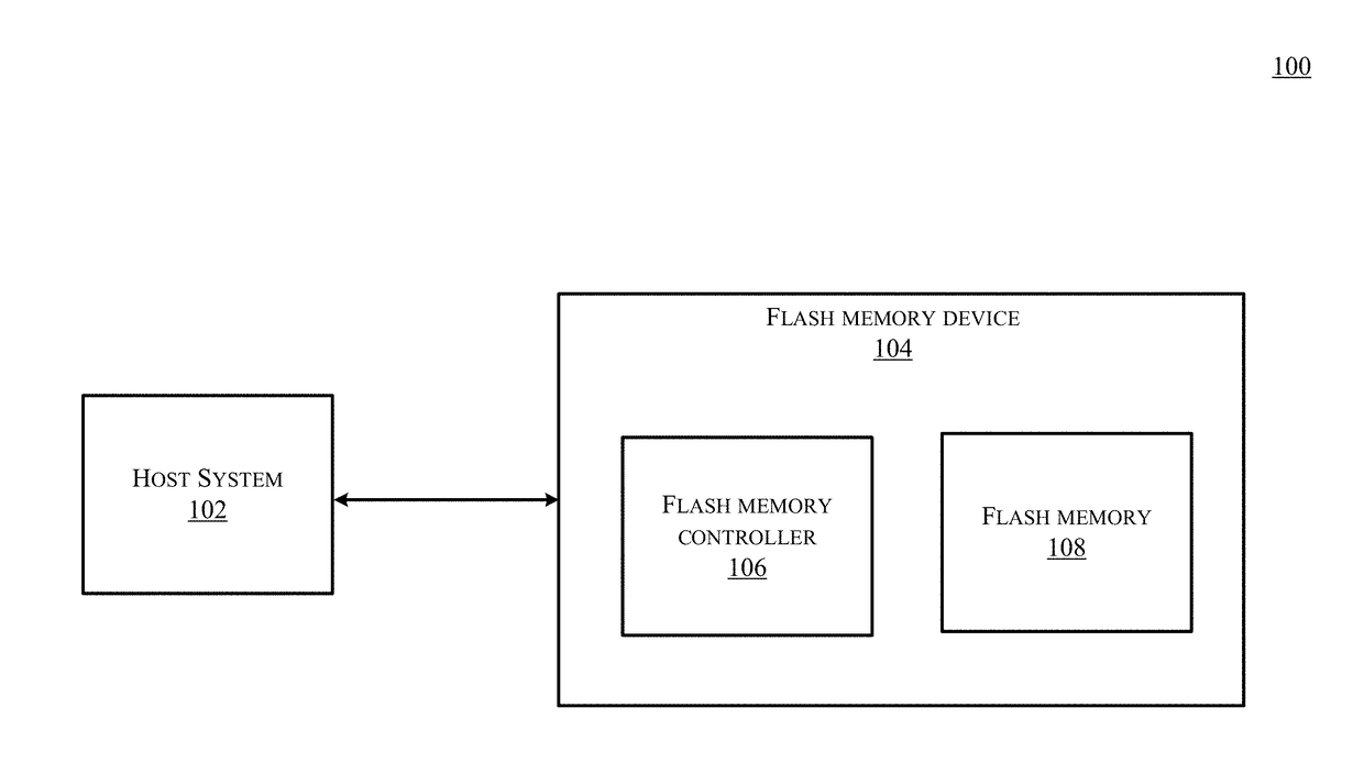
[0019]Certain aspects and embodiments of this disclosure are provided below. Some of these aspects and embodiments may be applied independently and some of them may be applied in combination as would be apparent to those of skill in the art. In the following description, for the purposes of explanation, specific details are set forth in order to provide a thorough understanding of embodiments. However, it will be apparent that various embodiments may be practiced without these specific details. The figures and description are not intended to be restrictive.

[0020]The ensuing description provides examples, and is not intended to limit the scope, applicability, or configuration of the disclosure. Rather, the ensuing description of the exemplary embodiments will provide those skilled in the art with an enabling description for implementing an exemplary embodiment. It should be understood that various changes may be made in the function and arrangement of elements without departing from ...


PUM


Abstract

Systems and methods are provided to detect a developed bad word-line of a flash memory. Embodiments provide an improved Background media scan (BGMS) process that can predict at the end of a block read if a word-line will potentially become bad with the use of the flash memory. Accordingly, data from the potentially bad block can be recovered and the block can be retired. The embodiments can minimize the need for the expensive chip-kill method.

Description

CROSS-REFERENCES TO RELATED APPLICATIONS[0001]This application is a non-provisional application and claims the benefit and priority of U.S. Provisional Application No. 62 / 320,377, filed on Apr. 8, 2016, titled “BACKGROUND MEDIA SCAN METHOD TO DETECT THE DEVELOPED BAD BLOCKS DURING SSD USAGE,” which is herein incorporated by reference in its entirety for all purposes.BACKGROUND OF THE INVENTION[0002]Non-volatile memory devices such as Solid State Drives (SSDs) are finding new applications in consumer electronics. For example, they are replacing Hard Disk Drives (HDDs), which typically comprise rapidly rotating disks (platters). Non-volatile memories, sometimes referred to as ‘flash memories’ or ‘flash memory devices’ (for example, NAND and NOR flash memory devices), are used in media storage, cameras, mobile phones, mobile computers, laptop computers, USB flash drives, etc. Non-volatile memory can provide a relatively reliable, compact, cost-effective, and easily accessible method of...

Claims


Application Information

Patent Timeline
Patent Type & Authority Applications(United States)
IPC IPC(8): G11C29/38G11C29/44G11C11/56
CPCG11C29/38G11C29/44G11C11/5628G11C11/5642A47G23/03A47L19/00A47L19/02A47L19/04F26B5/16G11C16/349G11C29/76
Inventor LI, HAIBOKIM, SANGSIKHAN, JUHYEON
Owner SK HYNIX INC
Why Eureka
Try Eureka