

Mapping table loading method, memory control circuit unit and memory storage apparatus
a memory storage apparatus and control circuit technology, applied in the direction of virtual memory details, instruments, computing, etc., can solve the problems of bandwidth waste and performance degradation and achieve the effect of improving the usage efficiency and performance of the memory storage apparatus
- Summary
- Abstract
- Description
- Claims
- Application Information
AI Technical Summary
Benefits of technology
Problems solved by technology
Method used
Image

Examples
first exemplary embodiment
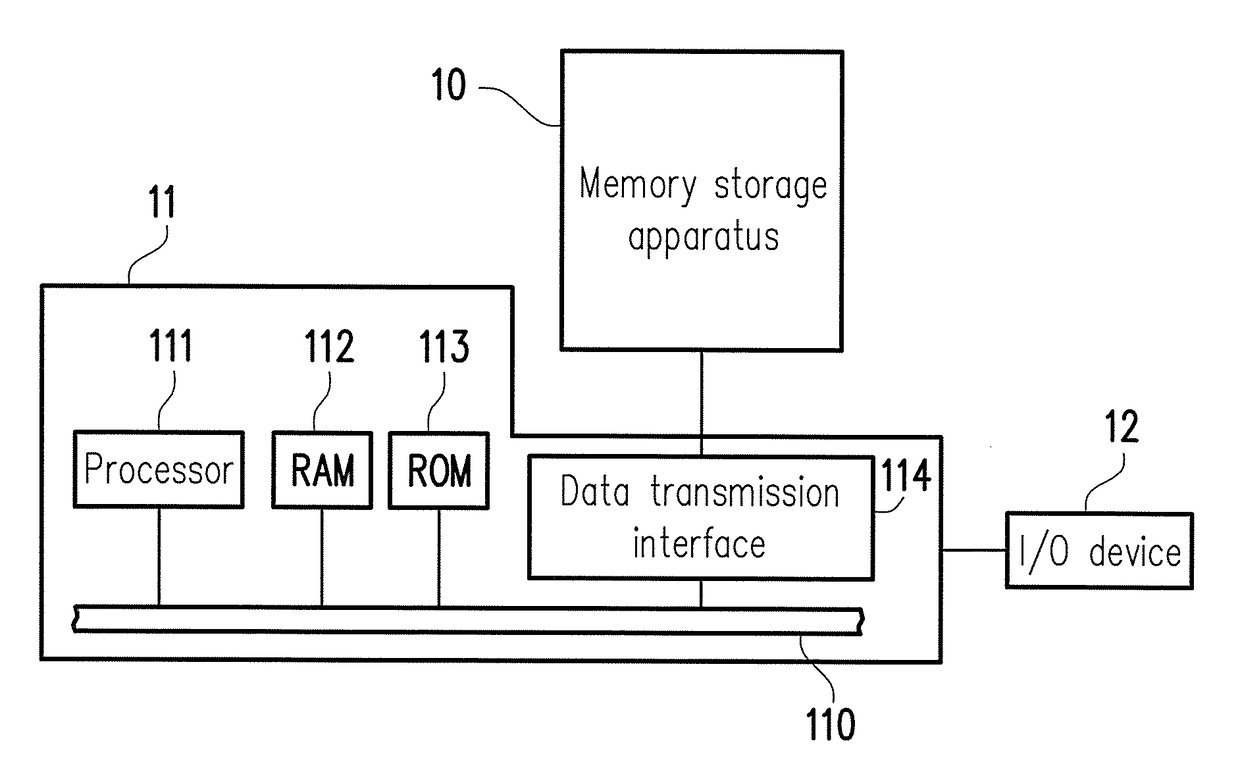
[0071]FIG. 9A and FIG. 9B are schematic diagrams illustrating a memory reading method according to a first exemplary embodiment. It should be stated that, in an exemplary embodiment, the memory control circuit unit 404 (or the memory management circuit 502) will establish a management table (not illustrated) in the buffer memory 508. The management table is configured to record the number of times one specific sub-logical address-physical address mapping table being loaded into the buffer memory 508 and used by the memory control circuit unit 404 (or the memory management circuit 502) (hereinafter, also known as a use count). In brief, the management table is configured to record a usage history of one specific sub-logical address-physical address mapping table.
[0072]Referring to FIG. 9A, in the exemplary embodiment of FIG. 9A, the memory control circuit unit 404 (or the memory management circuit 502) divides the buffer memory 508 into a first mapping table temporary storage area 50...
second exemplary embodiment
[0084]FIG. 10A and FIG. 10B are schematic diagrams illustrating a memory reading method according to a second exemplary embodiment. The exemplary embodiment of FIG. 10A includes similar process of loading the sub-logical address-physical address mapping table 810a according to the second command and recording the usage history of the sub-logical address-physical address mapping table 810a in the management table by the rewritable non-volatile memory module 406 after power-on in FIG. 9A, which is not repeated hereinafter. Referring to FIG. 10B in continuation to FIG. 10A, it is assumed that the host system 11 then issues the first command that corresponds to data stored in the logical address LBA(1) (hereinafter, also referred to as the first logical address), and the first command is a read command which instructs reading the data stored in the logical address LBA(1). After the memory control circuit unit 404 (or the memory management circuit 502) receives the first command from the...
third exemplary embodiment
[0088]FIG. 11A and FIG. 11B are schematic diagrams illustrating a memory reading method according to a third exemplary embodiment. The exemplary embodiment of FIG. 11A includes similar process of loading the sub-logical address-physical address mapping table 810a according to the second command and recording the usage history of the sub-logical address-physical address mapping table 810a in the management table in FIG. 9A, which is not repeated hereinafter. Referring to FIG. 11B in continuation to FIG. 11A, it is assumed that the host system 11 then issues the first command that corresponds to data stored in the logical address LBA(Z) (hereinafter, also referred to as the first logical address), and the first command is a read command which instructs reading the data stored in the logical address LBA(Z). After the memory control circuit unit 404 (or the memory management circuit 502) receives the first command from the host system 11, the memory control circuit unit 404 (or the memo...
PUM
 Abstract
Description
Claims
Application Information