Fingerprint identification method and device thereof

a fingerprint identification and fingerprint technology, applied in the field of fingerprint identification methods and fingerprint identification devices, can solve the problems of high cost of each chip, and difficulty in durability, so as to reduce the influence of ambient static electricity on the conventional capacitive fingerprint sensor, prevent a loophole of fingerprint identification, and increase the accuracy of identification

Active Publication Date: 2017-11-09
GINGY TECH
View PDF6 Cites 10 Cited by
  • Summary
  • Abstract
  • Description
  • Claims
  • Application Information

AI Technical Summary

Benefits of technology

[0008]Since a fake finger made of a silica gel material may exhibit deformation, fingerprint, and blood capillary characteristics similar to those of a real finger, such fake finger may easily pass a 3D fingerprint validation procedure of a fingerprint identification device. Accordingly, a fingerprint identification method and a fingerprint identification device are provided to solve the issue that the fake finger made of a silica gel material may easily pass the validation of the fingerprint identification device.
[0013]According to the embodiments of the invention, the photoelectronic sensor module receives the invisible light beam passing through the finger and the visible light beam reflected by the finger, and the gray-scale fingerprint image and the colored fingerprint image are simultaneously identified, so as to prevent a loophole of fingerprint identification and thus increase an accuracy of identification. Consequently, with the characteristics of being light and compact of the photoelectronic sensor module, the fingerprint identification device according to the embodiments of the invention may be applied in a handheld device, thereby improving on the issue that the conventional optical fingerprint identification device is too large to be used in the handheld device. In addition, by adopting a photoelectric separation-type sensing, the influence of ambient static electricity on the conventional capacitive fingerprint sensor may be reduced, and a sapphire substrate as protection in the conventional technology is no longer required. Therefore, a manufacturing cost may be significantly decreased.
[0014]Besides, in the case that blood capillaries are designed in a forged finger made of a silica gel material, by converting between chromaticity coordinates, the predetermined second skin color threshold of the second chromaticity coordinates may be used to validate again whether the blood capillaries are real. Accordingly, the loophole of fingerprint identification is eliminated by avoiding the forged fingerprint produced by utilizing the characteristic of skin color variation of the first chromaticity coordinates, thereby enhancing the capability of correctly distinguishing between real and forged fingerprints.

Problems solved by technology

However, the cost of the capacitive sensor is higher and the durability thereof remains challenged.
Thus, the cost of each chip is very high.
Furthermore, the capacitive sensor itself is an exposed semiconductor chip, so the chip surface may be eroded or the chip may generate static electricity because of the sweat on the finger and the acid / alkaline property thereof.
Thus, the durability and lifetime of the capacitive sensor may be significantly decreased.
However, such protective measure also increases the manufacturing cost.
However, due to its greater size and assembling complexities, it is difficult to install the optical fingerprint sensor inside the handheld device.
Thus, the fingerprint identification device is unable to determine whether the finger pressing thereupon is a real finger, which creates a loophole in identification.
Therefore, the capacitive fingerprint sensor may be affected by ambient static electricity and has a higher manufacturing cost, whereas the optical fingerprint sensor has a larger size and is not suitable for application in a handheld device.
Thus, how to design a fingerprint identification device free of influence of the ambient static electricity, having a smaller size and lower manufacturing cost, and capable of identifying the blood vessels of the real finger remains an issue to work on.

Method used


Image

  • Fingerprint identification method and device thereof
  • Fingerprint identification method and device thereof
  • Fingerprint identification method and device thereof

Examples


Embodiment Construction

[0027]Reference will now be made in detail to the present preferred embodiments of the invention, examples of which are illustrated in the accompanying drawings. Wherever possible, the same reference numbers are used in the drawings and the description to refer to the same or like parts.

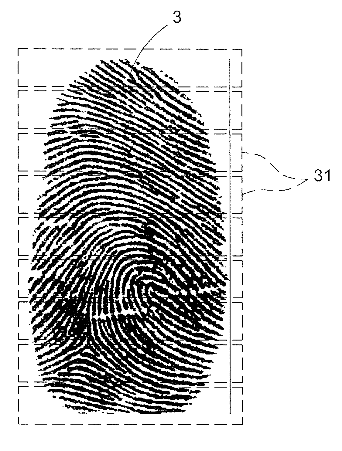
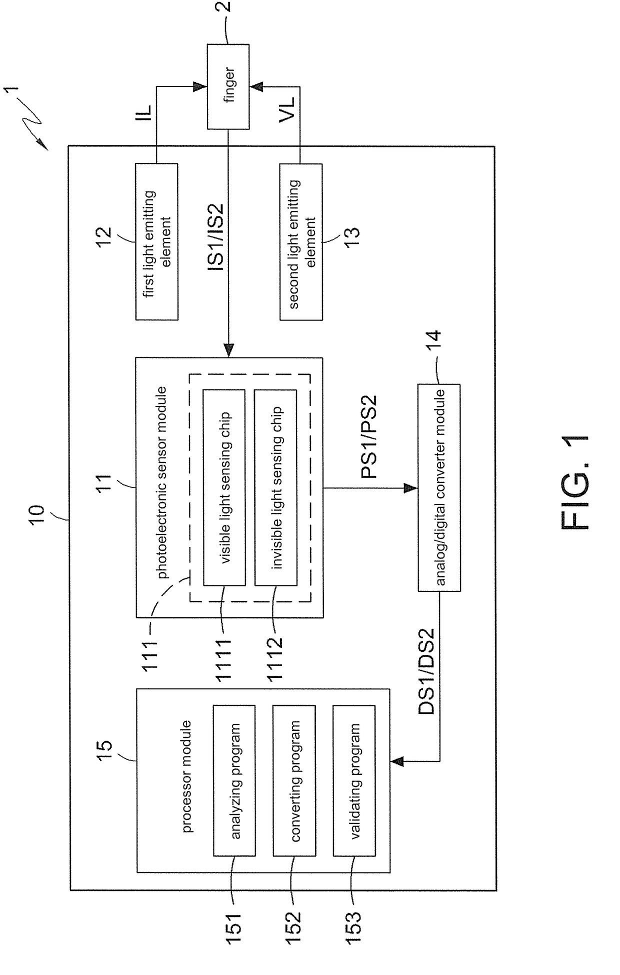
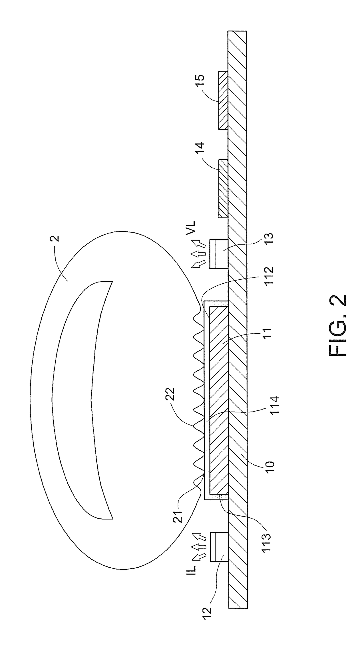
[0028]Referring to FIGS. 1 and 3, FIGS. 1 and 3 are respectively a schematic block view of a fingerprint identification device, a schematic framework of the fingerprint identification device, and a photoelectronic sensor module of the fingerprint identification device according to embodiments of the invention. The fingerprint identification device 1 includes a functional circuit board 10, a photoelectronic sensor module 11, at least one first light emitting element 12, at least one second light emitting element 13, an analog / digital converter module 14, and a processor module 15. The functional circuit board 10 provides the photoelectronic sensor module 11, and the first light emitting element 12 and...


PUM


Abstract

A fingerprint identification method is provided. The method includes steps as follows: having a finger press on a photoelectronic sensor module; respectively emitting an invisible light beam reflected to a photoelectronic sensor module after passing through the finger and a visible light beam reflected to the photoelectronic sensor module via a surface of the finger; generating, by the photoelectronic sensor module, photocurrent signals based on the visible light beam and the invisible light beam; respectively generating, by an analog / digital converter module, a first digital signal and a second digital signal based on the photocurrent signals; and outputting, by a processor module, the first digital signal as a gray-scale fingerprint image and a second digital signal as a colored fingerprint image. The invention also provides a fingerprint identification device performing the fingerprint identification method.

Description

BACKGROUND OF THE INVENTION1. Field of the Invention[0001]The invention relates to an identification method and an identification device, particularly relates to a fingerprint identification method and a fingerprint identification device.2. Description of Related Art[0002]Fingerprint identification, as the name indicates, relates to identification based on the unique fingerprint information on a finger of the human body. A conventional fingerprint identification device may include two elements. One of the components is a fingerprint sensor, which mainly serves to collect a complete fingerprint image. The other of the components is a fingerprint identification algorithm. After the fingerprint sensor at the front end collects the fingerprint image, the fingerprint identification algorithm may subsequently process the fingerprint image, extract features of the fingerprint, generate a fingerprint template, discard the original fingerprint image, and then perform fingerprint comparison.[...

Claims


Application Information

Patent Timeline
Patent Type & Authority Applications(United States)
IPC IPC(8): G06K9/00G06V10/143
CPCG06K9/00087G06K9/0004G06V40/1318G06V10/143H04N23/11G06V40/1365G06F18/00
Inventor WU, JEN-CHIEHHUNG, CHUN-LANG
Owner GINGY TECH
Why Eureka
Try Eureka