Electronic device

a technology of electronic devices and sealing resins, applied in the manufacture of printed circuits, printed circuit aspects, basic electric elements, etc., can solve the problems of reducing the area between the sealing resin and the heat radiation member, increasing the shrinkage factor of the sealing resin, and reducing the heat radiation efficiency, so as to achieve the effect of suppressing the decreas

Inactive Publication Date: 2017-11-16
DENSO CORP
View PDF3 Cites 6 Cited by
  • Summary
  • Abstract
  • Description
  • Claims
  • Application Information

AI Technical Summary

Benefits of technology

[0005]Another electronic device, which is not a conventional technology, may be considered. According to the electronic device, a circuit substrate is configured by a resin substrate. A heat-generation element mounted on one surface of the resin substrate is sealed with sealing resin. The sealing resin side is brought into contact with a heat radiation member to radiate heat of a circuit element from the sealing resin side. According to the electronic device, however, a mold shrinkage factor of the sealing resin extremely increases when the sealing resin is configured by sealing resin having the above linear expansion coefficient. In this case, the resin substrate side may bend into a convex shape. When the resin substrate side bends in this manner, only corners of the sealing resin of the electronic device contact the heat radiation member. In this condition, a contact area between the sealing resin and the heat radiation member decreases, thereby heat radiation efficiency may lower.
[0006]It is an object of the present disclosure to provide an electronic device capable of preventing lowering of heat radiation efficiency caused by bending.
[0010]Accordingly, it may be possible that the electronic device maintains the state of thermal connection between the opposite surface of the sealing resin and the heat radiation member while preventing a state that only corners of the sealing resin contact the heat radiation member in the temperature range from the normal temperature to the high temperature. In other words, it may be possible that the electronic device suppresses decrease in a contact area between the opposite surface and the heat radiation member in the temperature range from the normal temperature to the high temperature, thereby allowing radiation of heat generated by the heat-generation element to the heat radiation member. Accordingly, it may be possible to the electronic device suppresses lowering of heat radiation efficiency.

Problems solved by technology

According to the electronic device, however, a mold shrinkage factor of the sealing resin extremely increases when the sealing resin is configured by sealing resin having the above linear expansion coefficient.
In this condition, a contact area between the sealing resin and the heat radiation member decreases, thereby heat radiation efficiency may lower.

Method used


Image

  • Electronic device
  • Electronic device
  • Electronic device

Examples


first modified example

[0075](First Modified Example)

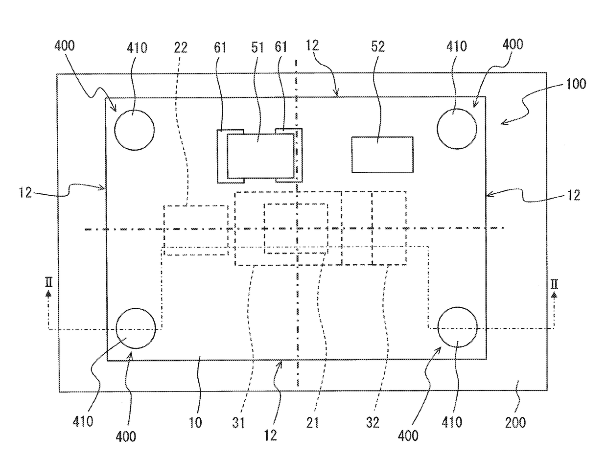
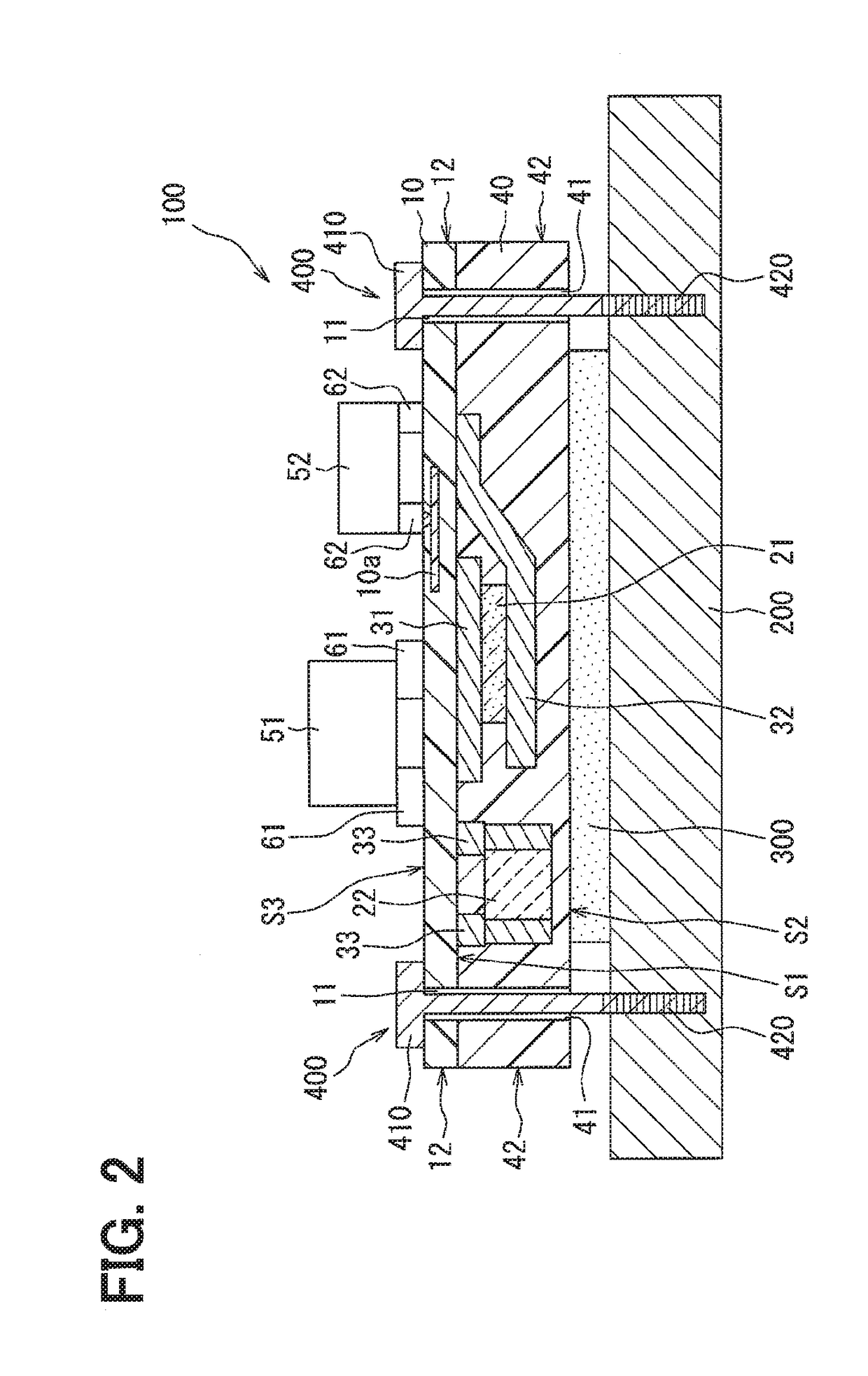
[0076]It may be preferable that the resin substrate 10 and the mold resin 40 of the mold package 100 have α1 and α2 for maintaining a cry bend in the first temperature range, and that al of the mold resin 40 be in a range of α1>10×10−6 / ° C. A cry bend state of the mold package 100 is also achievable by decreasing α1. However, when the difference between α1 and α2 of the mold package 100 increases, separation may be caused in the interface between the mold resin 40 and the circuit element sealed by the mold resin 40. Particularly, a of the chip capacitor 22 is generally smaller than each of α1 and α2. In addition, the chip capacitor 22 has a size larger than the size of the heat-generation element 21. Accordingly, when the difference between α1 and α2 increases in the mold package 100, a crack may be produced in the resin substrate 10, as well as separation caused in the interface between the chip capacitor 22 and the mold resin 40. More specifically, st...

second modified example

[0082](Second Modified Example)

[0083]It may be preferable that the mold package 100 satisfy a relationship (E1+10)≦E2 between a modulus of elasticity E1 of the mold resin 40 and a modulus of elasticity E2 of the resin substrate10, in addition to the relationship of the linear expansion coefficients described in the above embodiment. When the mold package 100 satisfies this relationship of modulus of elasticity, a cry bend is easily achieved in the first temperature range. The modulus of elasticity E1 of the mold resin 40 is approximately in a range from 10 GPa to 20 GPa. Accordingly, the modulus of elasticity E2 of the resin substrate 10 lies approximately in a range from 20 GPa to 30 GPa. The mold package 100 which includes the mold resin 40 and the resin substrate 10 having the foregoing relationship between the modulus of elasticity E1 and E2 easily produces a cry bend in the first temperature range.

[0084]The mold package 100 may he a mold package satisfying the relationship of t...

third modified example

[0085](Third Modified Example)

[0086]It may be preferable that the mold package 100 satisfy a condition that the thickness of the mold resin 40 is twice as large as the thickness of the resin substrate 10 or larger, in addition to the relationship of the linear expansion coefficients described in the above embodiment. When the thickness of the mold resin 40 of the mold package 100 is twice as large as the thickness of the resin substrate 10 or larger, a cry bend is easily produced in the first temperature range. For example, the mold package 100 may include the resin substrate 10 having a thickness of approximately 1 mm, and the mold resin 40 having a thickness of 2 mm or longer.

[0087]The mold package 100 may be a mold package satisfying the relationship of the thicknesses described in the third modified example in addition to the relationship of the linear expansion coefficients described in the first modified example, and the relationship of the modulus of elasticity described in t...


PUM


Abstract

An electronic device includes: a resin substrate that includes insulation resin on which wiring made of conductive material is provided; a heat-generation element that is a circuit element mounted on a first surface of the resin substrate, and is operated to generate heat; and a sealing resin that is provided on the first surface, and seals the heat-generation element. An opposite surface of the sealing resin opposite to a surface of the sealing resin in contact with the first surface is thermally connected to a heat radiation member and mounted on the heat radiation member. Each of the resin substrate and the sealing resin has a bend shape convex toward the opposite surface when each of surrounding temperatures is a normal temperature and has a linear expansion coefficient for maintaining a bend shape convex toward the opposite surface when each of the surrounding temperatures is a high temperature.

Description

CROSS REFERENCE TO RELATED APPLICATIONS[0001]The present application is based on Japanese Patent Application No. 2014-253382 filed on Dec. 15, 2014, the disclosure of which is incorporated herein by reference.TECHNICAL FIELD[0002]The present disclosure relates to an electronic device that includes a circuit element mounted on a resin substrate, the circuit element being sealed with sealing resin.BACKGROUND ART[0003]A hybrid integrated circuit device disclosed in Patent Literature 1 is an example of a conventional electronic device. The hybrid integrated circuit device includes components such as a circuit substrate made of aluminum, a circuit element fixed to a conductive pattern provided on a surface of the circuit substrate, and sealing resin made of thermosetting resin that covers by transfer molding with exposure of at least a rear surface of the circuit substrate through the sealing resin. A thermal expansion coefficient of the sealing resin of the hybrid integrated circuit dev...

Claims


Application Information

Patent Timeline
Patent Type & Authority Applications(United States)
IPC IPC(8): H01L23/40H01L23/28H01L23/367H05K1/02
CPCH01L23/40H01L23/28H05K1/0209H01L23/367H05K2201/062H01L23/29H01L2924/0002H01L23/145H01L23/3121H01L23/3737H01L23/4006H01L23/42H05K3/284H01L2023/405H05K2201/068H05K2201/09136H05K2201/10166H05K2201/10409H01L2924/00
Inventor YAMAGISHI, TETSUTONAGAYA, TOSHIHIROTAKENAKA, MASAYUKIHIRAMITSU, SHINJI
Owner DENSO CORP
Why Eureka
Try Eureka