Photovoltaic module and a method for producing the same

a photovoltaic module and photovoltaic technology, applied in the direction of sustainable manufacturing/processing, climate sustainability, semiconductor devices, etc., can solve the problems of layer needs, low output voltage per cell, transparent conductive oxide, etc., to reduce the resistance of the contact finger, the effect of reducing the length of the contact finger

Inactive Publication Date: 2017-11-16
SOLIBRO RES AB
View PDF6 Cites 0 Cited by
  • Summary
  • Abstract
  • Description
  • Claims
  • Application Information

AI Technical Summary

Benefits of technology

[0022]The first hole and the second hole may be adjacent to each other. This means that the length of the contact finger may be as short as possible, whereby the resistance in the contact finger decreases. Another advantage with this is that efficient manufacturing may become possible.
[0023]A first center point of the first hole and a second center point of the second hole may lie on a center line perpendicular to the first groove and the second groove. This has the effect that the length of the contact finger may be as short as possible and thereby the resistance may be minimized.
[0024]The contact finger may be a metal finger arranged in parallel with the center line. This may allow a short metal finger that decreases the resistance of the contact finger.
[0025]The photovoltaic stack may comprise a CIGS structure with a ZAO top contact. The ZAO top layer provides a top contact with low resistance, and if this is combined with contact fingers the thickness of the ZAO layer may be reduced, thereby allowing more light to enter the CIGS stack.

Problems solved by technology

Due to the inherent nature of a photovoltaic cell, the available output voltage per cell is too low to be useful.
A well-known problem associated with monolithic integration is that due to the routing a part of the area of the photovoltaic cell does not contribute to the photovoltaic conversion.
Another loss in the monolithic interconnect is that the top transparent conductive oxide (TCO) layer needs to be relatively conductive to minimize resistive losses.
However, by making the TCO quite conductive, it also absorbs more light which lowers the performance of the solar cell.
Due to the limiting performance of the TCO's, there is a relatively large loss of performance of the solar cell in this layer.

Method used


Image

  • Photovoltaic module and a method for producing the same
  • Photovoltaic module and a method for producing the same
  • Photovoltaic module and a method for producing the same

Examples


first embodiment

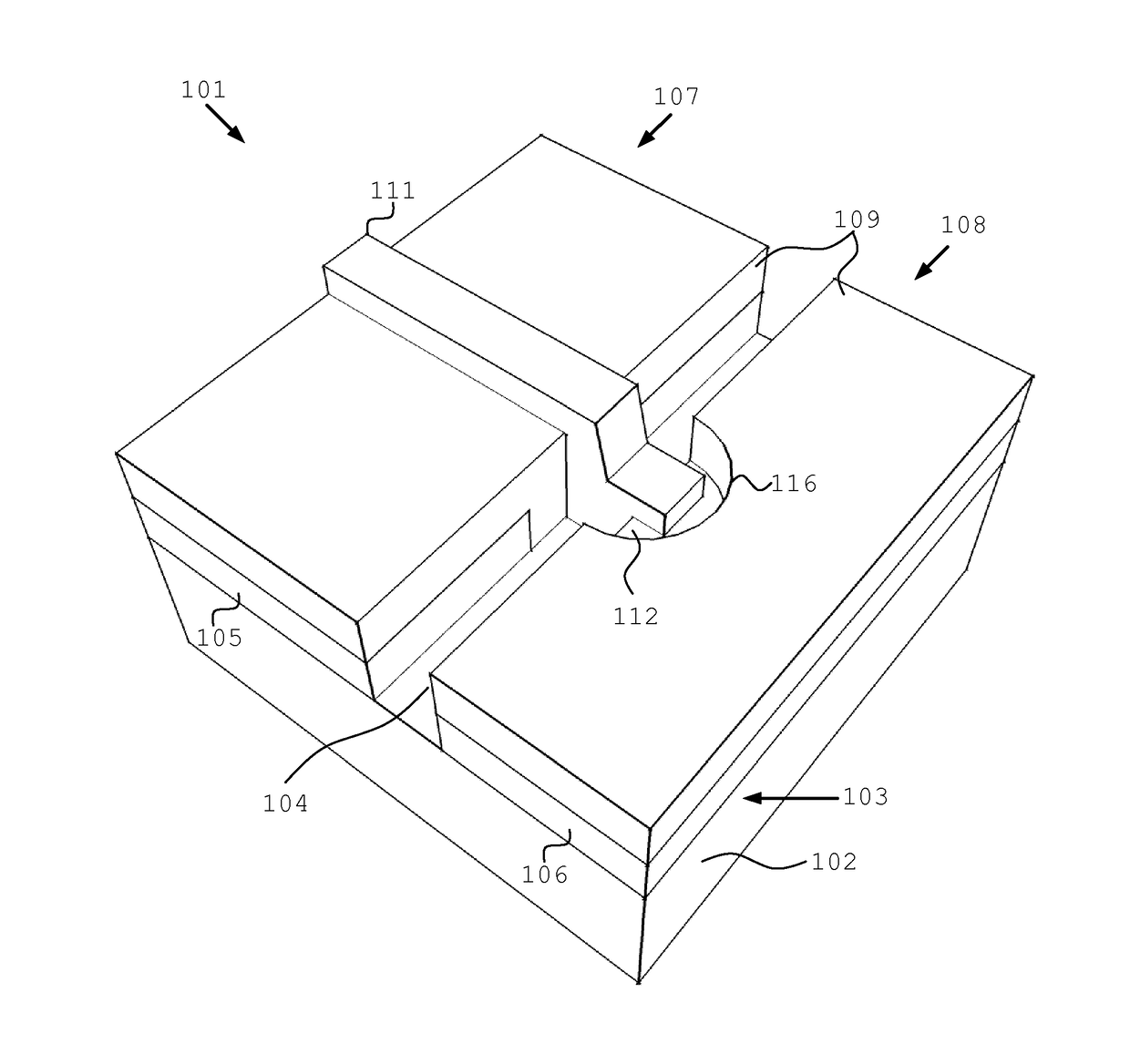
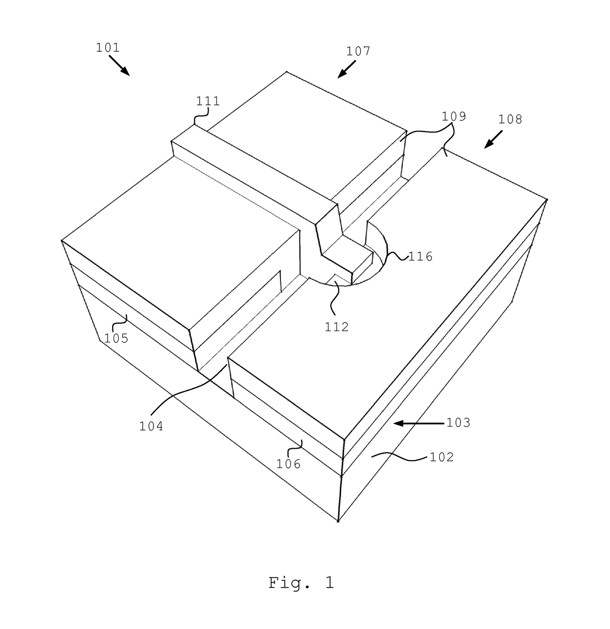
[0036]the present invention, a photovoltaic module, generally designated 101, is shown in FIG. 1. The photovoltaic module 101 comprises a substrate 102. The substrate 102 may be a sheet of glass or another suitable material that provides sufficient isolation and suitable surface properties.

[0037]A contact layer 103 is arranged on the substrate 102. The contact layer 103 may comprise a layer of molybdenum (Mo) that has been deposited on the substrate 102. A first gap 104 is provided in the contact layer 103. This first gap 104 forms and defines a first contact 105 and a second contact 106 in the contact layer 103. The first contact 105 is a bottom contact for a first photovoltaic cell 107, and the second contact 106 is a bottom contact for a second photovoltaic cell 108. The first gap 104 extends through the thickness of the contact layer 103 such that the first contact 105 and the second contact 106 are isolated from each other.

[0038]A photovoltaic stack 109 is provided on each of t...

third embodiment

[0062]The photovoltaic stack 109 of the third embodiment may comprise a photovoltaic structure according to the above description and as shown in FIG. 8.

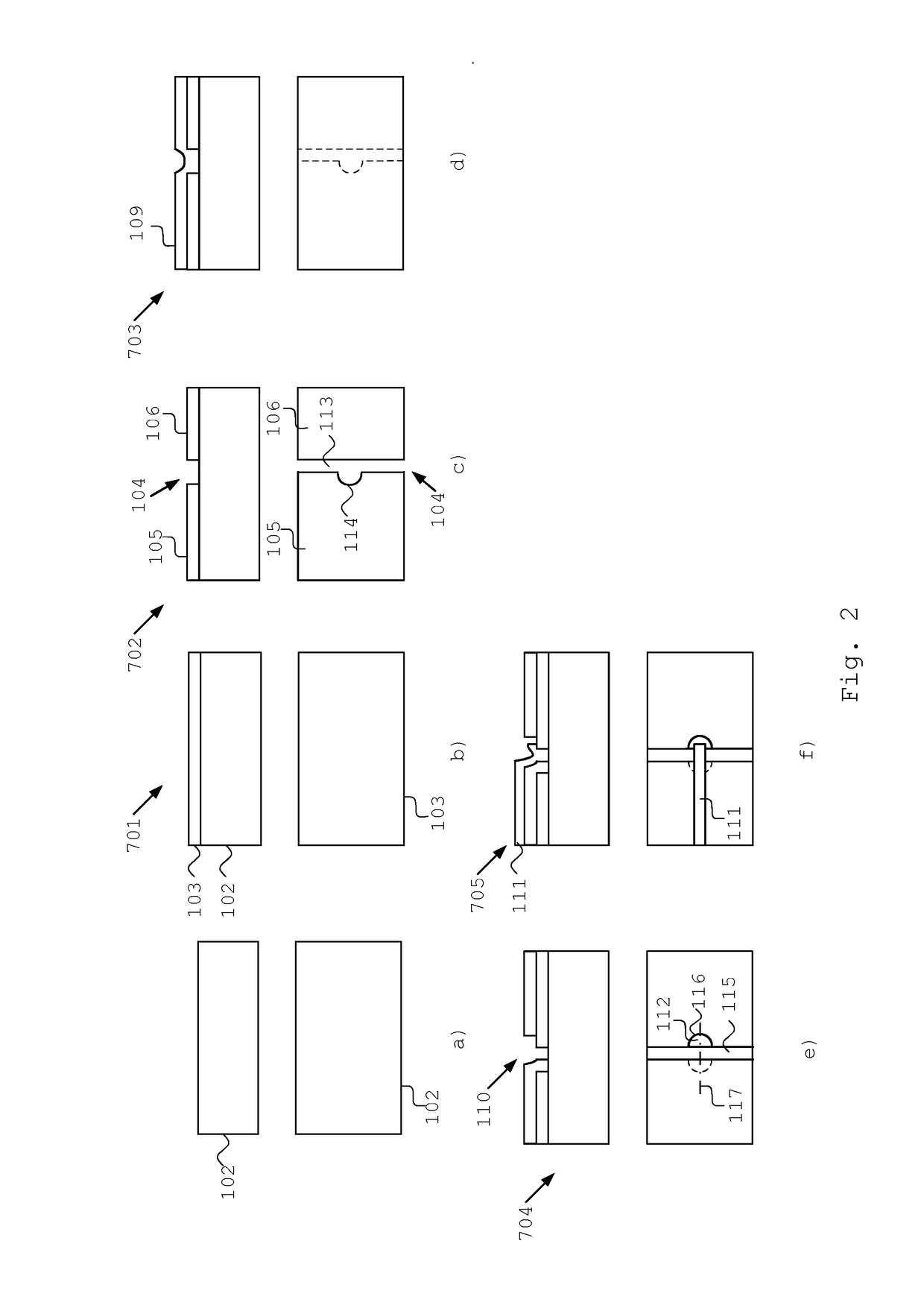
[0063]In FIG. 6a)-f) a method for producing a photovoltaic module 101′ according to the third embodiment is disclosed. Features of the third embodiment that relate to features of the first embodiment by function have been given the same number indexing, but with a prime.

[0064]This method starts with a substrate 102, which may be a sheet of glass or a metal strip for example.

[0065]In FIG. 6b, on the substrate 102′ is a contact layer 103′ deposited by means of for example sputtering, evaporation or the like. The contact layer 103′ may be a layer of molybdenum (Mo).

[0066]FIG. 6c) discloses a process for forming the first gap 104′ by means of scribing, laser etching, milling or the like. The first gap 104′ defines a first contact 105 and a second contact 106 that are electrically isolated from each other. In this embodiment the first ga...


PUM


Abstract

A photovoltaic module and a method for producing such modules is presented in which the resistance of the interconnects between neighboring photovoltaic cells is minimized and the dead-area is also minimized. This is achieved by routing the interconnects, in form of a finger, from a top contact of a first photovoltaic cell to a bottom contact of a second photovoltaic cell. The interconnect is isolated from the bottom contact of the first photovoltaic cell by means of the photovoltaic stack and the interconnect is connected to the bottom contact of the second photovoltaic cell in an opening of the photovoltaic stack.

Description

TECHNICAL FIELD[0001]The present invention relates to a photovoltaic module, as well as a method for producing such a photovoltaic module. In particular, the present invention relates to a photovoltaic module with photovoltaic cells, which are connected by means of contact fingers, as well as a method for producing such photovoltaic modules.BACKGROUND[0002]Due to the inherent nature of a photovoltaic cell, the available output voltage per cell is too low to be useful. Therefore, in order to achieve a useful output voltage, usually several photovoltaic cells are commonly connected in series. This series connection is for thin film solar cells usually performed by routing the top contact of a photovoltaic cell to a bottom contact of a neighboring photovoltaic cell. This way of connecting cells is often referred to as “monolithic integration”. A well-known problem associated with monolithic integration is that due to the routing a part of the area of the photovoltaic cell does not cont...

Claims


Application Information

Patent Timeline
Patent Type & Authority Applications(United States)
IPC IPC(8): H01L31/0465H01L31/0749H01L31/05H01L31/18H01L31/02
CPCH01L31/0465H01L31/0749H01L31/02021H01L31/0504H01L31/1876Y02E10/541Y02P70/50
Inventor LUNDBERG, OLLE
Owner SOLIBRO RES AB
Why Eureka
Try Eureka