Encapsulated Circuit Module, And Production Method Therefor

Inactive Publication Date: 2017-11-30
MEIKO ELECTRONICS CO LTD
View PDF0 Cites 16 Cited by
  • Summary
  • Abstract
  • Description
  • Claims
  • Application Information

AI Technical Summary

Benefits of technology

[0022]As described above, different metals have different abilities to shield electric and magnetic fields. In the present invention, the shield layer includes two layers of different metals, i.e., the first metal covering layer comprising a first metal having an excellent shielding property against an electric field and being copper or iron, and the second metal covering layer comprising a second metal having an excellent shielding property against a magnetic field and being nickel, thereby achieving a better shielding effect against the electric and magnetic fields that create electromagnetic waves. Since electromagnetic waves are waves (vibrational energy) formed as a result of the changes in electric and magnetic fields in a space, by shielding them individually, the shielding effect against electromagnetic waves becomes synergistically large. In the present invention, the first metal covering layer and the second metal covering layer are each thicker than 5 μm. The reason for this is as follows. In the present invention, the former serves to shield the electric field and the latter serves to shield the magnetic field. It has been found in the studies made by the present applicant th

Problems solved by technology

Some electronic components are vulnerable to electromagnetic waves.
Moreover, some other electronic components are vulnerable to electromagnetic waves and others emit electromagnetic waves.
When, however, a box is used, the height from the substrate to the upper surface of the box often becomes relatively great, and the thickness of the circuit module thus tends to be great.
Where boxes are used, it takes

Method used


Image

  • Encapsulated Circuit Module, And Production Method Therefor
  • Encapsulated Circuit Module, And Production Method Therefor
  • Encapsulated Circuit Module, And Production Method Therefor

Examples


Embodiment Construction

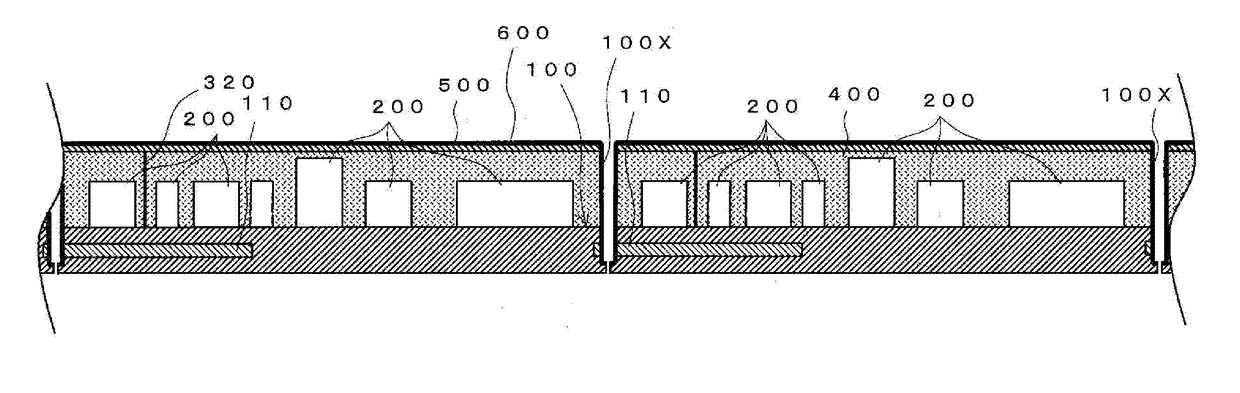
[0025]The present inventor provides the following method to solve the aforementioned problems. The following method is an example of a method of manufacturing the aforementioned encapsulated circuit module.

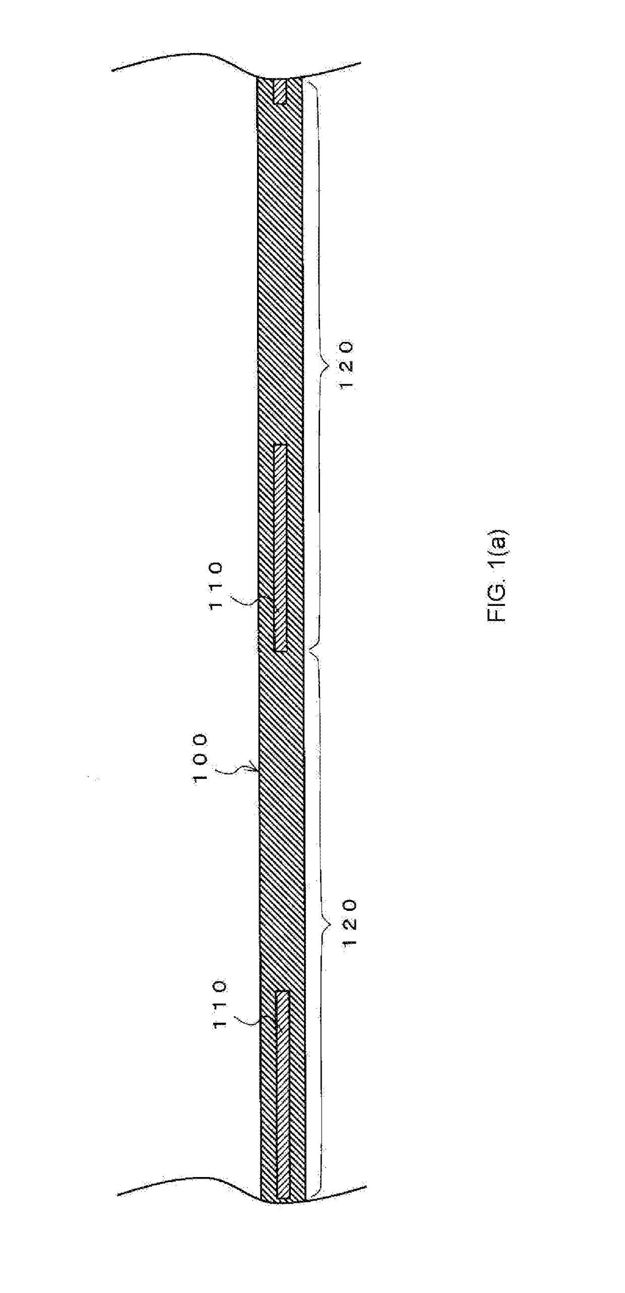
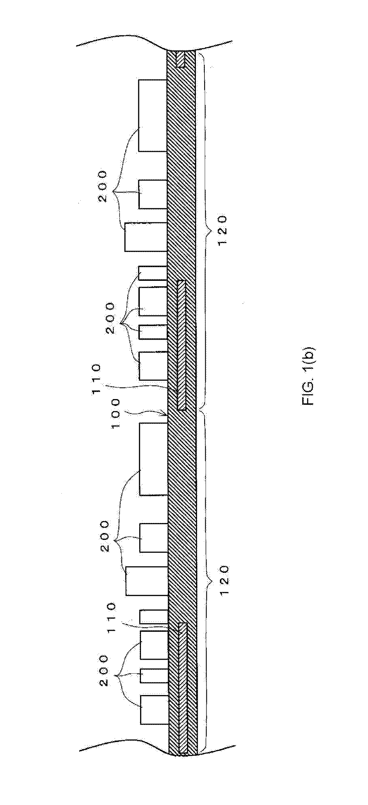
[0026]The method is a method of manufacturing encapsulated circuit modules including: a first covering step for entirely covering a surface of a substrate with a first resin together with electronic components and curing the first resin, the surface of the substrate having a plurality of contiguous assumed sections, each of the sections having at least one of the electronic components mounted thereon, the substrate having a ground electrode; a snicking step for removing a predetermined width of the first resin and the substrate to a predetermined depth of the substrate, the predetermined width including a boundary between the adjacent assumed sections; a shield layer-forming step for forming a metal shield layer on a surface of the first resin and side surfaces of the first resin ...


PUM


Abstract

To improve, in an encapsulated circuit module having a metal shield layer covering a surface of a resin layer containing filler, a shielding property of the shield layer against electromagnetic waves.
The encapsulated circuit module has a substrate 100 on which electronic components are mounted, covered with a first resin 400. A surface of the first resin 400 is covered with a shield layer 600 including a first metal covering layer 610 made of copper or iron and a second metal covering layer 620 made of nickel. Each of the first metal covering layer 610 and the second metal covering layer 620 is thicker than 5 μm.

Description

TECHNICAL FIELD[0001]The present invention relates to encapsulated circuit modules.BACKGROUND ART[0002]Encapsulated circuit modules are known.[0003]Encapsulated circuit modules include a substrate having wiring (such as a printed wiring board), electronic components mounted so as to be electrically connected with the wiring of the substrate, and a resin covering the substrate together with the electronic components. By covering the electronic components with the resin, encapsulated circuit modules can provide protection for electronic components and protection of electrical contacts between the electronic components and the wiring of the substrate.[0004]Encapsulated circuit modules include electronic components as described above. Some electronic components are vulnerable to electromagnetic waves. Other electronic components emit electromagnetic waves.[0005]In many situations where an encapsulated circuit module is actually used, the encapsulated circuit module is combined with othe...

Claims


Application Information

Patent Timeline
IPC IPC(8): H05K3/28H05K1/18H05K9/00H05K3/00H05K3/12H05K3/18
CPCH05K3/284H05K9/0088H05K3/0044H05K3/0052H05K9/0022H05K1/181H05K3/181H05K3/12H05K2201/10371H05K2201/10522H05K2203/1316H05K2203/1322H05K2203/1327H01L24/97H01L2924/1815H01L2924/3025H01L23/3121H01L21/561H01L23/552H01L23/66H01L2223/6677H05K9/0024
Inventor MIWA, SATORU
Owner MEIKO ELECTRONICS CO LTD
Why Eureka
Try Eureka