Atomic layer etching using a boron-containing gas and hydrogen fluoride gas

a technology of hydrogen fluoride and boron-containing gas, which is applied in the direction of hydrogen fluoride, boron/boride, electrical equipment, etc., can solve the problems of becoming a significant challenge in accurately controlling the etching of fine features, self-limiting and atomic scale processing methods such as ale becoming a necessity

Active Publication Date: 2018-02-15
TOKYO ELECTRON LTD
View PDF5 Cites 13 Cited by
  • Summary
  • Abstract
  • Description
  • Claims
  • Application Information

AI Technical Summary

Problems solved by technology

As device feature size continues to scale it is becoming a significant challenge to accurately control etching of fine features.
In this regards, self-limiting and atomic scale processing methods such as ALE are becoming a necessity.

Method used


Image

  • Atomic layer etching using a boron-containing gas and hydrogen fluoride gas
  • Atomic layer etching using a boron-containing gas and hydrogen fluoride gas
  • Atomic layer etching using a boron-containing gas and hydrogen fluoride gas

Examples


Embodiment Construction

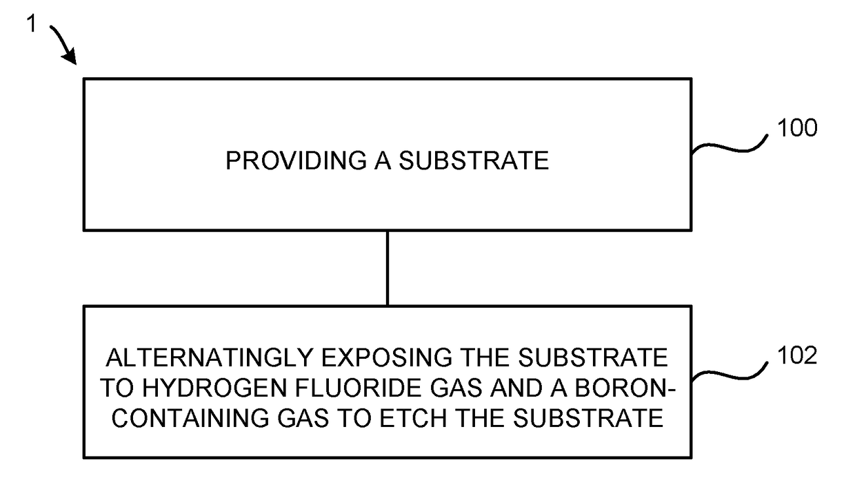
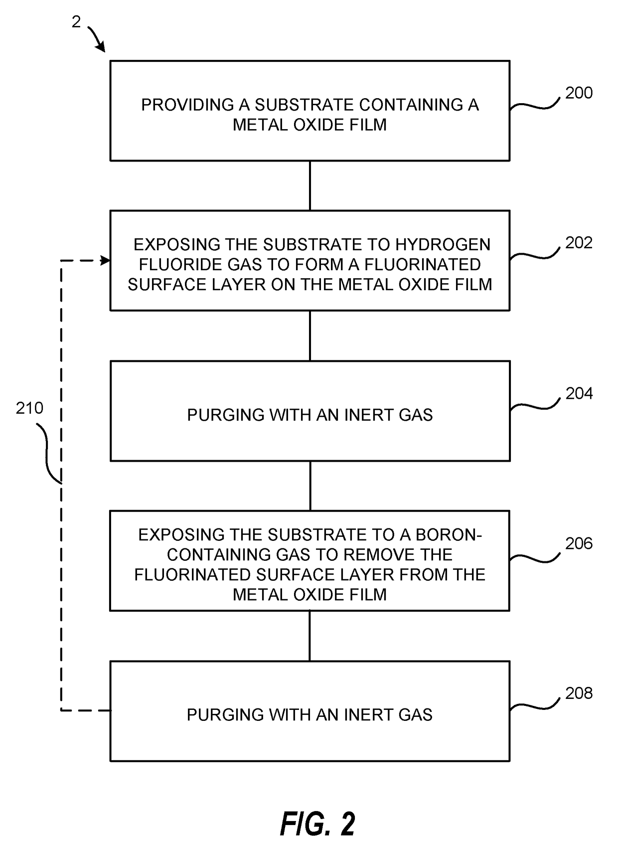
[0015]Developing advanced technology for advanced semiconductor technology nodes presents an unprecedented challenge for manufacturers of semiconductor devices, where these devices will require atomic-scale manufacturing control of etch variability. ALE is viewed by the semiconductor industry as an alternative to conventional continuous etching. ALE is a substrate processing technique that removes thin layers of material using sequential self-limiting reactions and is considered one of the most promising techniques for achieving the required control of etch variability necessary in the atomic-scale era.

[0016]ALE is often defined as a film etching technique that uses sequential self-limiting reactions. The concept is analogous to atomic layer deposition (ALD), except that removal occurs in place of a second adsorption step, resulting in layer-by-layer material removal instead of addition. The simplest ALE implementation consists of two sequential steps: surface modification (1) and r...


PUM


Abstract

Embodiments of the invention provide a method for atomic layer etching (ALE) of a substrate. According to one embodiment, the method includes providing a substrate, and exposing the substrate to hydrogen fluoride (HF) gas and a boron-containing gas to etch the substrate. According to another embodiment, the method includes providing a substrate containing a metal oxide film, exposing the substrate to HF gas to form a fluorinated surface layer on the metal oxide film, and exposing the substrate to a boron-containing gas to remove the fluorinated surface layer from the metal oxide film. The exposures may be repeated at least once to further etch the metal oxide film.

Description

CROSS-REFERENCE TO RELATED APPLICATIONS[0001]This application is related to and claims priority to U.S. Provisional Patent Application Ser. No. 62 / 373,232 filed on Aug. 10, 2016, the entire contents of which are herein incorporated by reference.FIELD OF INVENTION[0002]The present invention relates to the field of semiconductor manufacturing and semiconductor devices, and more particularly, to atomic layer etching (ALE) of a substrate using a boron-containing gas and hydrogen fluoride (HF) gas.BACKGROUND OF THE INVENTION[0003]As device feature size continues to scale it is becoming a significant challenge to accurately control etching of fine features. For highly scaled nodes 10 nm and below, devices require atomic scaled fidelity or very tight process variability. There is significant impact on device performance due to variability. In this regards, self-limiting and atomic scale processing methods such as ALE are becoming a necessity.SUMMARY OF THE INVENTION[0004]A method is provid...

Claims


Application Information

Patent Timeline
Patent Type & Authority Applications(United States)
IPC IPC(8): H01L21/311
CPCH01L21/31116C01B7/191C01B35/02C01B35/06H01L21/31122H01L21/3065H01L21/0228H01L21/02046H01L21/31138
Inventor CLARK, ROBERT D.TAPILY, KANDABARA N.
Owner TOKYO ELECTRON LTD
Why Eureka
Try Eureka