Goa circuit applied for in cell type touch display panel

a cell-type touch display and circuit technology, applied in the field of display technology, can solve the problem of large and achieve the effect of promoting the working efficiency of the goa circuit and reducing the loading of the ic for the signal process in the touch scan stag

Active Publication Date: 2018-03-01
WUHAN CHINA STAR OPTOELECTRONICS TECH CO LTD
View PDF0 Cites 6 Cited by
  • Summary
  • Abstract
  • Description
  • Claims
  • Application Information

AI Technical Summary

Benefits of technology

[0064]The benefits of the present invention are: the present invention provides a GOA circuit applied for the In Cell type touch display panel. By redesigning the output buffer module, the third transmission gate comprising the second P-type thin film transistor and the third N-type thin film transistor, the first P-type thin film transistor and the fourth N-type thin film transistor are added in the output buffer module, and the touch control signal and the inverted touch control signal are introduced to control the working status of the output buffer module. Thus, in the normal display stage, the third transmission gate is activated, and the first, the fourth thin film transistors are deactivated, and the output buffer module normally outputs the gate scan driving signal. However, in the touch scan stage, the third transmission gate is deactivated, and the first, the fourth thin film transistors are activated, and the gate scan driving signal output end is floating, and the outputted gate scan driving signal appears in a high impedance state, and similarly jumps between high, low voltage levels along with that the touch scan driving signal jumps between high, low voltage levels, and the loading of the IC for the signal process in the touch scan stage can be reduced to promote the working efficiency of the GOA circuit.

Problems solved by technology

Such work of the touch scan panel requires performing waveform process to the gate scan driving signal in the touch scan stage with the Integrated Circuit (IC), and results in larger loading of the IC.

Method used


Image

  • Goa circuit applied for in cell type touch display panel
  • Goa circuit applied for in cell type touch display panel
  • Goa circuit applied for in cell type touch display panel

Examples


Embodiment Construction

[0076]For better explaining the technical solution and the effect of the present invention, the present invention will be further described in detail with the accompanying drawings and the specific embodiments.

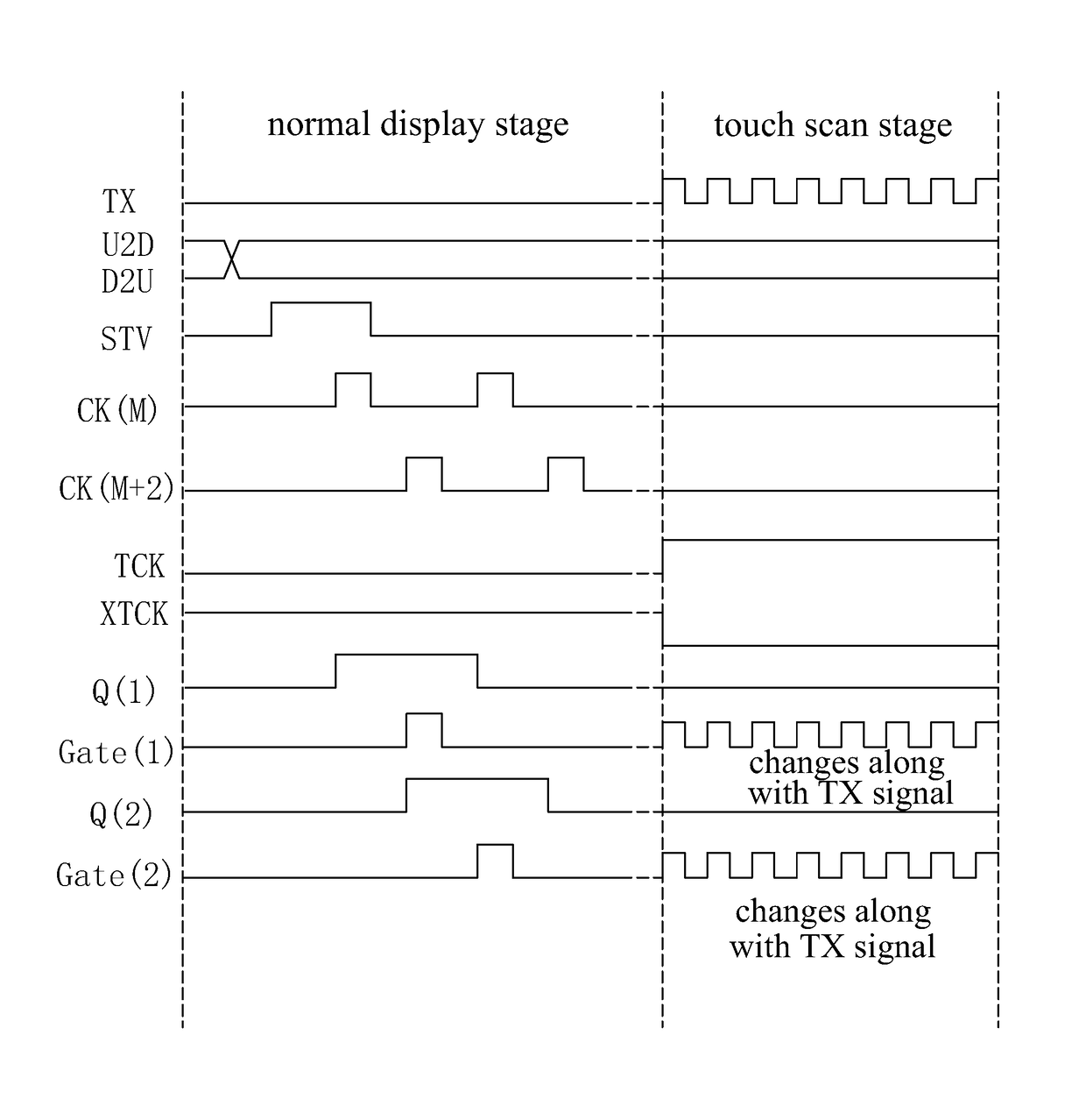
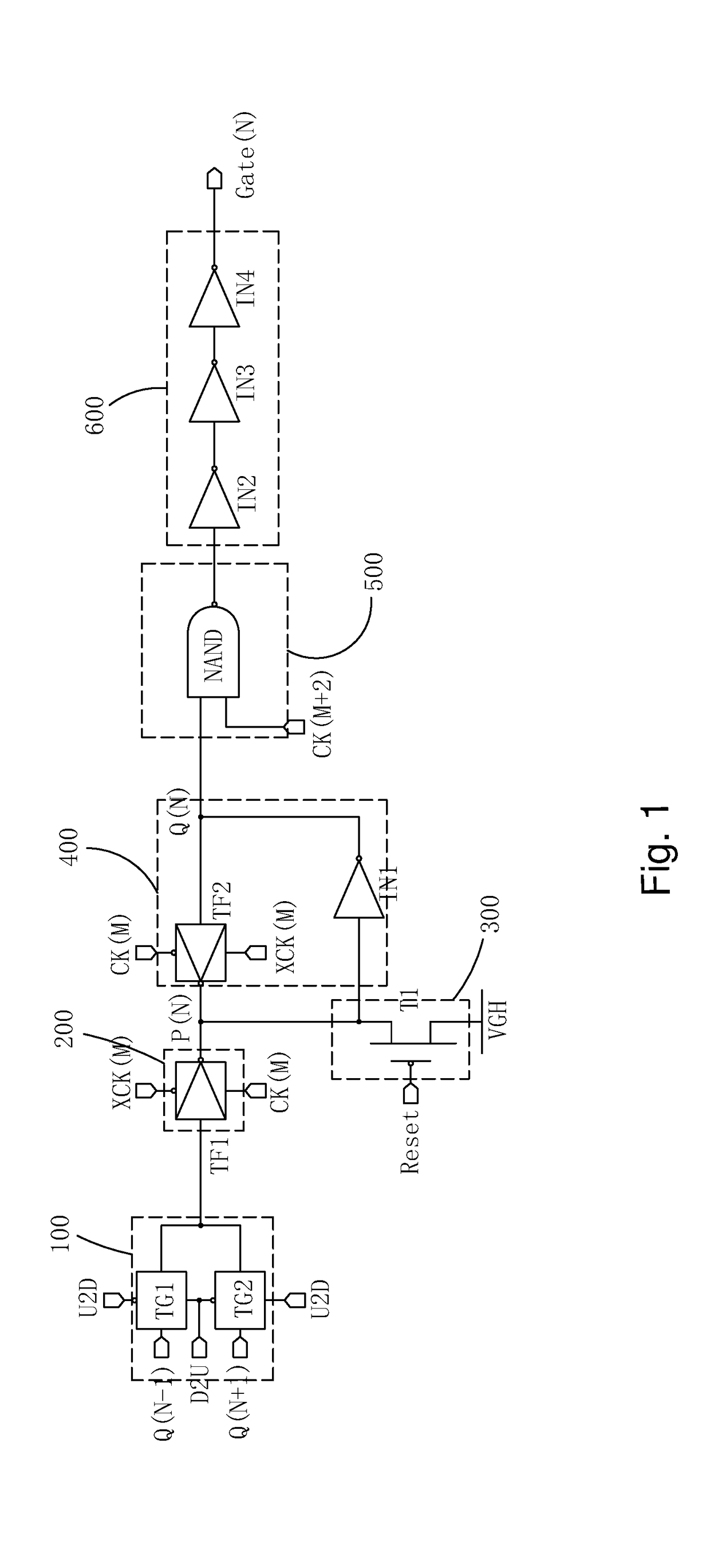
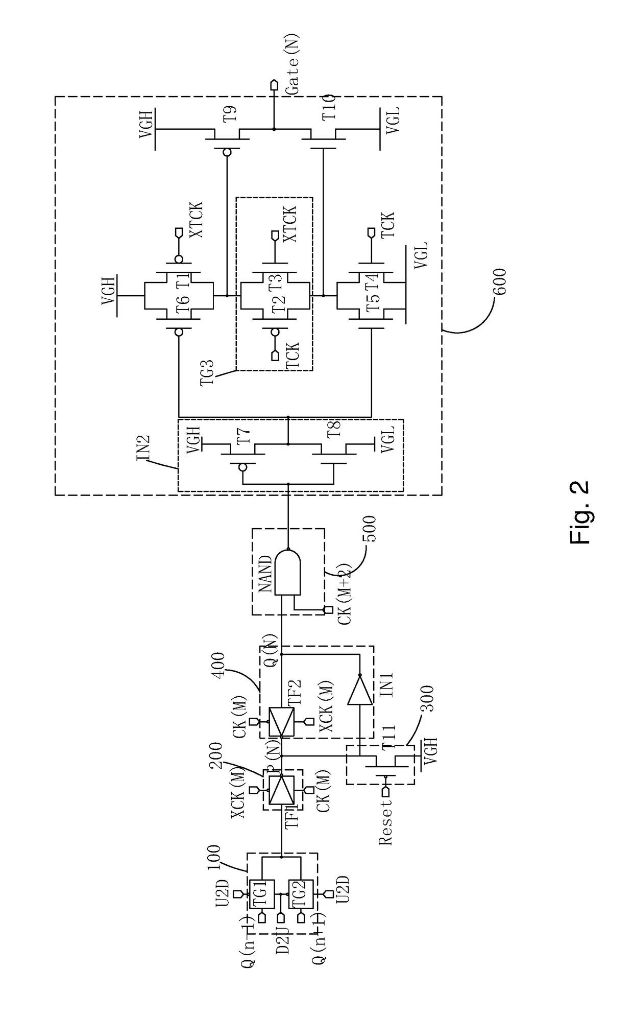
[0077]Please refer to FIG. 2 and FIG. 5, the present invention provides a GOA circuit applied for an In Cell type touch display panel, comprising GOA units of a plurality of stages which are cascade coupled, and the GOA unit of each stage comprises: a forward-backward scan control module 100, a control input module 200, a reset module 300, a latch module 400, a NAND gate signal process module 500 and an output buffer module 600.

[0078]N is set to be a positive integer, and except the GOA unit of the first stage and the GOA unit of the last stage, in the GOA unit of the Nth stage:

[0079]the forward-backward scan control module 100 comprises: a first transmission gate TG1, and a low voltage level control end of the first transmission gate TG1 receives a first direct current contro...


PUM


Abstract

The present invention provides a GOA circuit applied for the In Cell type touch display panel. The third transmission gate (TG3) comprising the second P-type thin film transistor (T2) and the third N-type thin film transistor (T3), the first P-type thin film transistor (T1) and the fourth N-type thin film transistor (T4) are added in the output buffer module (600), and the touch control signal (TCK) and the inverted touch control signal (XTCK) are introduced to control the working status of the output buffer module (600). Thus, in the touch scan stage, the third transmission gate (TG3) is deactivated, and the first, the fourth thin film transistors (T1, T4) are activated, and the gate scan driving signal output end (Gate(N)) is floating, and similarly jumps between high, low voltage levels along with that the touch scan driving signal jumps between high, low voltage levels.

Description

FIELD OF THE INVENTION[0001]The present invention relates to a display technology field, and more particularly to a GOA circuit applied for an In Cell type touch display panel.BACKGROUND OF THE INVENTION[0002]The GOA (Gate Driver on Array) technology, i.e. the array substrate row driving technology is to utilize the array manufacture process of the Thin Film Transistor (TFT) liquid crystal display to manufacture the gate driving circuit on the Thin Film Transistor array substrate for realizing the driving way of scanning the gates row by row. It possesses advantages of reducing the production cost and realizing the panel narrow frame design, and is utilized by many kinds of displays. The GOA circuit has two basic functions: the first is to output the scan driving circuit for driving the gate lines in the panel to activate the TFTs in the display areas and to charge the pixels; the second is the shift register function. When the output of one scan driving signal is accomplished, the ...

Claims


Application Information

Patent Timeline
Patent Type & Authority Applications(United States)
IPC IPC(8): G06F3/041G09G3/36
CPCG11C19/28G09G2310/0283G09G2300/0408G02F1/13454G09G2310/0286G09G3/3659G09G3/3677G09G2310/0291G09G2310/08G09G2310/0289G06F3/0412G02F1/13338G09G2354/00G06F3/04184G09G3/36G06F3/04166
Inventor CHEN, CAIQINZHAO, MANG
Owner WUHAN CHINA STAR OPTOELECTRONICS TECH CO LTD
Why Eureka
Try Eureka