Photoelectric conversion device and imaging system
a technology of conversion device and image, applied in the field of photoelectric conversion device, can solve the problems of degrading image quality and image quality not necessarily improving, and achieve the effect of reducing both white spots and image lag, and high image quality
- Summary
- Abstract
- Description
- Claims
- Application Information
AI Technical Summary
Benefits of technology
Problems solved by technology
Method used
Image
Examples
Embodiment Construction
[0015]An embodiment of the present concept will now be described with reference to the drawings. In the following description and the drawings, the same reference numerals refer to the same parts throughout the drawings. The description of the same parts designated by the same reference numerals throughout the drawings may be omitted.
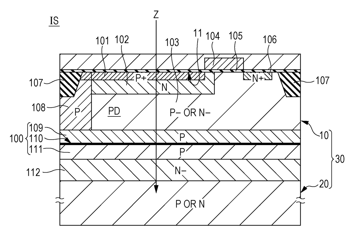
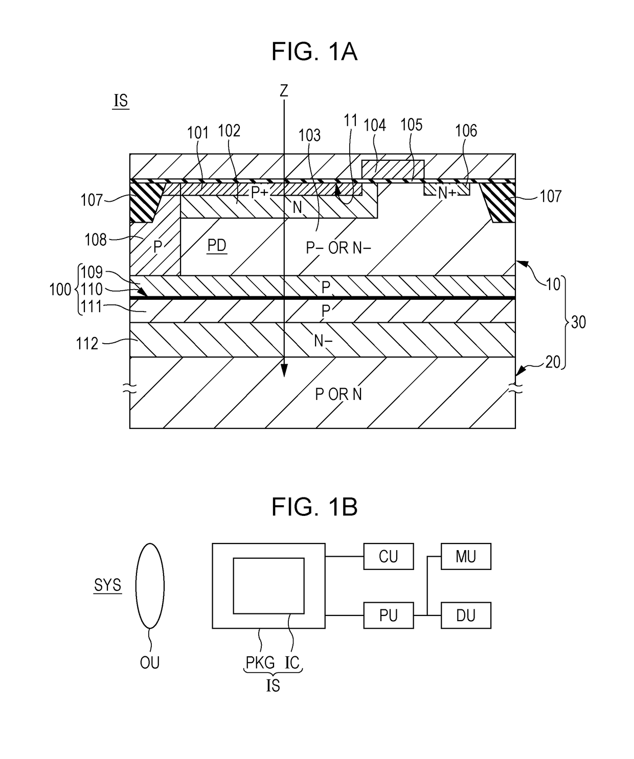
[0016]FIG. 1A illustrates a cross section of the photoelectric conversion portion PD of a photoelectric conversion device IS.
[0017]The photoelectric conversion device IS includes a silicon layer 10. The silicon layer 10 is disposed on a base 20. The silicon layer 10 may be a monocrystalline silicon layer (epitaxial layer) epitaxially grown on the base 20. Since the base 20 is made of monocrystalline silicon, the silicon layer 10 and the base 20 are collectively referred to as a silicon substrate 30. The silicon layer 10 has a thickness of, for example, 5 μm to 20 μm, and the base 20 has a thickness of, for example, 20 μm to 8000 μm.
[0018]The silicon lay...
PUM
 Abstract
Description
Claims
Application Information


