Eureka AIR delivers breakthrough ideas for toughest innovation challenges, trusted by R&D personnel around the world.

Integrated circuit designing system and a method of manufacturing an integrated circuit

Active Publication Date: 2018-03-08
SAMSUNG ELECTRONICS CO LTD
View PDF2 Cites 3 Cited by
  • Summary
  • Abstract
  • Description
  • Claims
  • Application Information

AI Technical Summary

Benefits of technology

The invention relates to a method and system for designing and manufacturing integrated circuits. The method includes placing cells, reordering pins in a cell, and performing a routing operation on the cells to produce a layout for the integrated circuit. The system includes a processor and memory to perform the placement and routing operations and produce the integrated circuit. The technical effect of the invention is to improve the efficiency and accuracy of integrated circuit design and manufacture.

Problems solved by technology

Further, in the case that multi-patterning technology, such as double patterning technology (DPT) and triple patterning technology (TPT), is used in the microfabrication process, local congestion may occur near some of the pins in a cell.

Method used


Image

  • Integrated circuit designing system and a method of manufacturing an integrated circuit
  • Integrated circuit designing system and a method of manufacturing an integrated circuit
  • Integrated circuit designing system and a method of manufacturing an integrated circuit

Examples


Embodiment Construction

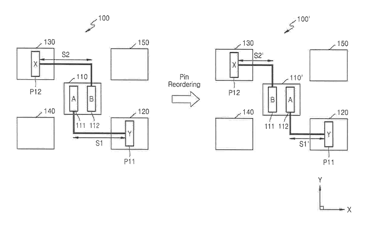
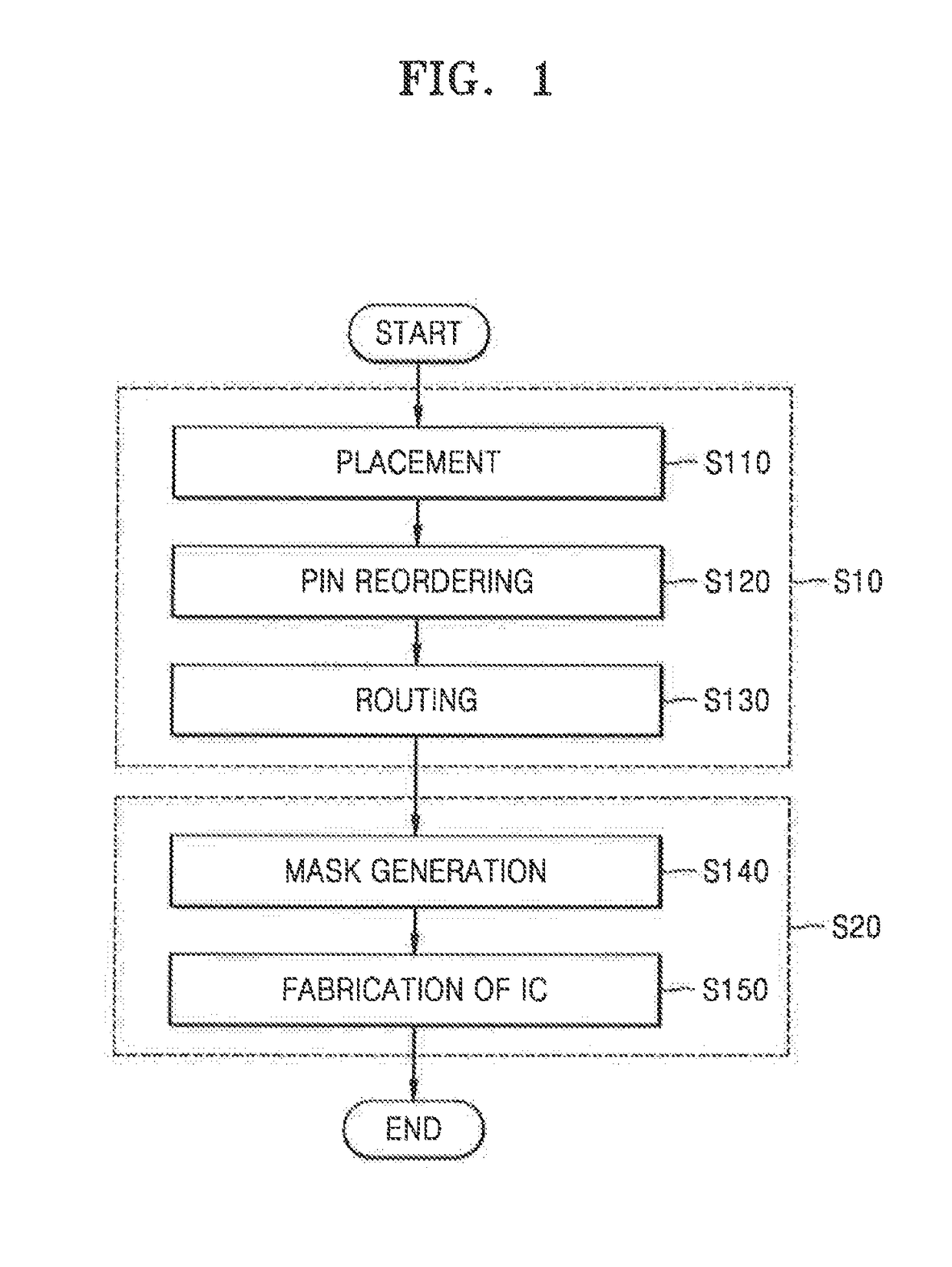
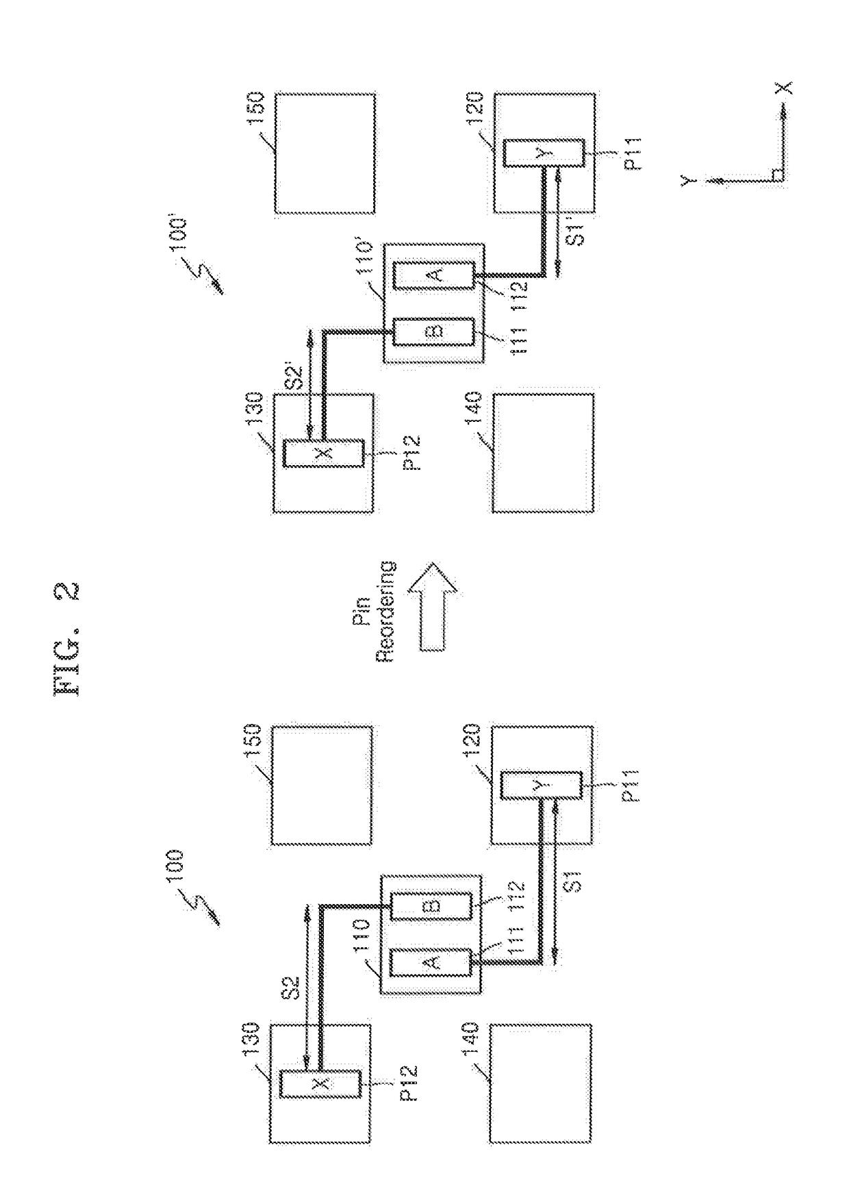
[0023]FIG. 1 is a flowchart illustrating a method of manufacturing an integrated circuit, according to an exemplary embodiment of the inventive concept.

[0024]Referring to FIG. 1, a method of manufacturing an integrated circuit (IC) according to the present embodiment may include an IC designing process S10 and an IC manufacturing process (S20). The IC designing process S10 may be performed to prepare a layout for ICs and may include operations S110, S120, and S130, which are performed using an IC design tool. Here, the IC design tool may be a program including a plurality of instructions to be executed by a processor. Accordingly, the IC designing process S10 may be a computer implemented method of designing ICs. The IC manufacturing process S20 may be an operation of manufacturing a semiconductor device including ICs, based on a designed layout, and may be performed in a semiconductor process module.

[0025]An IC may be defined by a plurality of cells and may be designed using a cell...


PUM


Abstract

A method of manufacturing an integrated circuit may include placing cells, based on input data defining the integrated circuit, performing a pin reordering operation on a plurality of pins in a first cell of the cells, based on physical information regarding the pins in the first cell, wherein the physical information is determined based on the placement of the cells, performing a routing operation on the cells after the pin reordering operation, and manufacturing the integrated circuit, based on a layout produced by the routing operation.

Description

CROSS-REFERENCE TO RELATED APPLICATION[0001]This application claims priority under 35 U.S.C. §119 to Korean Patent Application No. 10-2016-0115714, filed on Sep. 8, 2016, in the Korean Intellectual Property Office, the disclosure of which is incorporated by reference herein in its entirety.TECHNICAL FIELD[0002]The inventive concept relates to an integrated circuit, and in particular, to a system of designing an integrated circuit, a computer-implemented method of designing an integrated circuit, and a method of manufacturing an integrated circuit.DISCUSSION OF RELATED ART[0003]Due to increasing demand for high-performance semiconductor chips, there exists an increase in a pin density of a cell. To make such high-performance chips, a semiconductor microfabrication process is used. However, the number of design rules of a cell increase in the semiconductor microfabrication process. Further, in the case that multi-patterning technology, such as double patterning technology (DPT) and tr...

Claims


Application Information

Patent Timeline
IPC IPC(8): H01L21/66G03F7/20H01L21/02
CPCH01L22/20G03F7/70483H01L21/02035G03F7/70616G06F30/394G06F30/39H01L27/0207H01L23/525H01L23/5226H01L2027/11875G06F30/3947G06F30/396
Inventor KIMKIM, HYUNG-OCKNOH, WOO YOUNGCHOI, JUNG YUN
Owner SAMSUNG ELECTRONICS CO LTD
Why Eureka
Eureka Blog
Learn More