

Semiconductor device and method of manufacturing semiconductor device
- Summary
- Abstract
- Description
- Claims
- Application Information
AI Technical Summary
Benefits of technology
Problems solved by technology
Method used
Image

Examples
Embodiment Construction
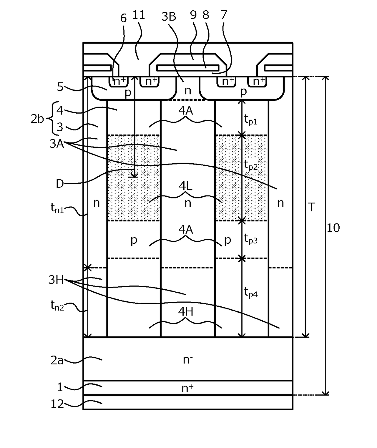
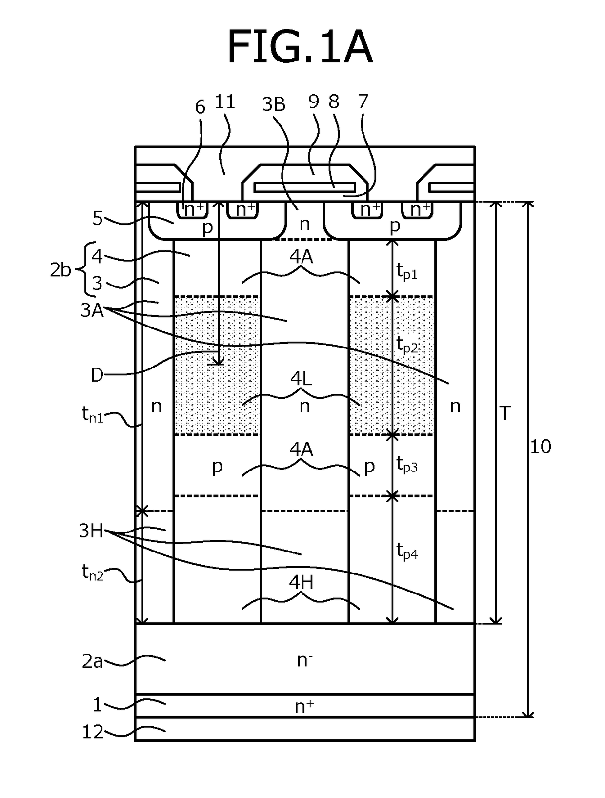
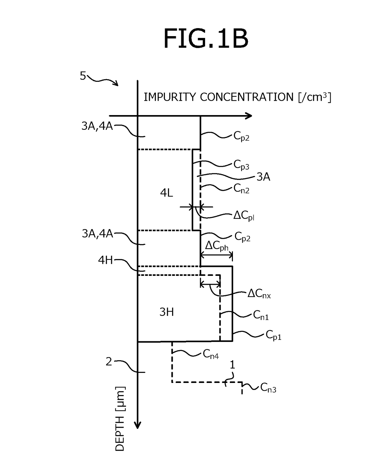
[0033]Embodiments of a semiconductor device and a method of manufacturing a semiconductor device according to the present invention will be described in detail with reference to the accompanying drawings. In the present description and accompanying drawings, layers and regions prefixed with n or p mean that majority carriers are electrons or holes. Additionally, + or − appended to n or p means that the impurity concentration is higher or lower, respectively, than layers and regions without + or −. In the description of the embodiments below and the accompanying drawings, main portions that are identical will be given the same reference numerals and will not be repeatedly described.
[0034]A structure of the semiconductor device according to a first embodiment will be described taking a planar gate superjunction MOSFET (hereinafter, SJ-MOSFET) as an example. FIGS. 1A, 1B, and 1C are diagrams of constituent regions of the semiconductor device according to the first embodiment. FIG. 1A d...
PUM
 Abstract
Description
Claims
Application Information