Amoled pixel driving circuit and pixel driving method

a driving circuit and pixel technology, applied in the field of display technology, can solve problems such as many defects

Active Publication Date: 2018-04-12
SHENZHEN CHINA STAR OPTOELECTRONICS TECH CO LTD
View PDF4 Cites 5 Cited by
  • Summary
  • Abstract
  • Description
  • Claims
  • Application Information

AI Technical Summary

Benefits of technology

[0058]The benefits of the present invention are: the present invention provides an AMOLED pixel driving circuit and a pixel driving method which utilize the 6T1C structure driving circuit, wherein the third thin film transistor is located between a drain of the first thin film transistor and a power source positive voltage, and controls a light emitting time of the organic light emitting diode by receiving a light emitting control signal, and the fourth thin film transistor is located between a gate of the first thin film transistor and a power source negative voltage, and controls writing the power source negative voltage to the gate of the first thin film transistor by receiving an electrical property recovery control signal, and the fifth thin film transistor and the sixth thin film transistor are electrically coupled to the drain and a source of the first thin film transistor, respectively, and control writing a reference negative voltage to the drain and the source of the first thin film transistor with the electrical property recovery control signal, and a difference value of the power source negative voltage and the reference negative voltage is set to be negative, which can perform recovery to the electrical property drift of the drive thin film transistor after the organic light emitting diode finishes light emitting to stable the light emitting brightness of the organic light emitting diode and promote the display quality.

Problems solved by technology

The structure of the pixel driving circuit shown in FIG. 1 is simpler and does not have the compensation function, and thus many defects exist.

Method used


Image

  • Amoled pixel driving circuit and pixel driving method
  • Amoled pixel driving circuit and pixel driving method
  • Amoled pixel driving circuit and pixel driving method

Examples


Embodiment Construction

[0066]For better explaining the technical solution and the effect of the present invention, the present invention will be further described in detail with the accompanying drawings and the specific embodiments.

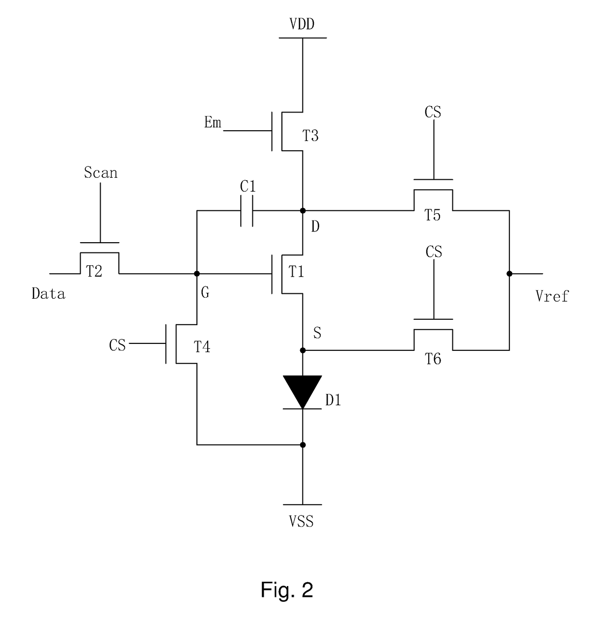
[0067]Please refer to FIG. 2 and FIG. 3 at the same time. The present invention first provides an AMOLED pixel driving circuit, and the AMOLED pixel driving circuit utilizes a 6T1C structure, and comprises: a first thin film transistor T1, a second thin film transistor T2, a third thin film transistor T3, a fourth thin film transistor T4, a fifth thin film transistor T5, a sixth thin film transistor T6, a first capacitor C1 and an organic light emitting diode D1.

[0068]The second thin film transistor T2 is employed to be a switch thin film transistor, and a gate thereof receives a scan signal Scan, and a source receives a data signal Data, and a drain is electrically coupled to the gate G of the first thin film transistor T1; a gate of the third thin film transistor T3 receives...


PUM


Abstract

The present invention provides an AMOLED pixel driving circuit and a pixel driving method which utilize the 6T1C structure driving circuit, wherein the fourth thin film transistor (T4) is located between a gate (G) of the first thin film transistor (T1) and a power source negative voltage (VSS), and controls writing the power source negative voltage (VSS) to the gate (G) of the first thin film transistor (T1) by receiving an electrical property recovery control signal (CS), and the fifth thin film transistor (T5) and the sixth thin film transistor (T6) are electrically coupled to a drain (D) and a source (S) of the first thin film transistor (T1), respectively, and control writing a reference negative voltage (Vref) to the drain (D) and the source (S) of the first thin film transistor (T1) with the electrical property recovery control signal (CS).

Description

FIELD OF THE INVENTION[0001]The present invention relates to a display technology field, and more particularly to an AMOLED pixel driving circuit and a pixel driving method.BACKGROUND OF THE INVENTION[0002]The Organic Light Emitting Display (OLED) possesses many outstanding properties of self-illumination, low driving voltage, high luminescence efficiency, short response time, high clarity and contrast, near 180° view angle, wide range of working temperature, applicability of flexible display and large scale full color display. The OLED is considered as the most potential display device.[0003]The OLED can be categorized into two major types according to the driving methods, which are the Passive Matrix OLED (PMOLED) and the Active Matrix OLED (AMOLED), i.e. two types of the direct addressing and the Thin Film Transistor (TFT) matrix addressing. The AMOLED comprises pixels arranged in array and belongs to active display type, which has high lighting efficiency and is generally utiliz...

Claims


Application Information

Patent Timeline
Patent Type & Authority Applications(United States)
IPC IPC(8): G09G3/3233H01L27/32
CPCG09G3/3233H01L27/3262H01L27/3265G09G2320/045H10K59/1213H10K59/1216
Inventor HAN, BAIXIANG
Owner SHENZHEN CHINA STAR OPTOELECTRONICS TECH CO LTD
Why Eureka
Try Eureka