Integrated Circuit Calibration Architecture

a technology of integrated circuits and calibration architectures, applied in the field of electronic circuits, can solve the problems of difficult to obtain accurate calibration measurements of such performance in the assembled final system, experience constructive interference, and other signals at other angles experience destructive interference, and achieve the effects of accurate calibration of rf ics, simple testing environment, and lower frequency

Active Publication Date: 2018-05-10
PSEMI CORP
View PDF2 Cites 12 Cited by
  • Summary
  • Abstract
  • Description
  • Claims
  • Application Information

AI Technical Summary

Benefits of technology

[0007]Advantages of various embodiments of the invention include a calibration architecture that enables accurate calibration of RF ICs used in transceiver RF systems in a relatively simple testing environment that is done by direct connection (as opposed to over-the-air) at significantly lower frequencies. Accordingly, environmental factors in the test set-up that alter, shield, attenuate, distort, or otherwise affect transmitted and received over-the-air test signals are eliminated or significantly mitigated by using such direct connections.
[0008]While direct connection via switchable internal calibration paths provides for accurate calibration of RF IC transceiver circuits, in some embodiments, internal switches and antenna mutual coupling enable over-the-air calibration, alone or in combination with direct signal coupling via internal calibration paths. Such embodiments thus allow even more complete calibration that takes into account the RF signal path from transceiver to transceiver through over-the-air test signals.
[0009]Periodic self-calibration of an RF IC in accordance with the present invention can be performed after initial factory calibration, so that adjustments in desired performance parameters can be made while such an IC is embedded within a final system, and thus take into account the actual usage environment (including, for example, temperature, electrically “noisy” circuitry, parasitic electromagnetic coupling, etc.). Periodic self-calibration also allows re-characterization of such an RF IC to take into account component degradation due to age or other factors.

Problems solved by technology

Beamforming combines transmit / receive elements in a phased array in such a way that signals at particular angles experience constructive interference while other signals at other angles experience destructive interference.
However, accurate calibration measurements of such performance are difficult to obtain in an assembled final system where all measurements need to be done “over the air”, meaning actually transmitting a signal (which may be varied over a band of frequencies) from one transceiver through an antenna and receiving that signal in a different transceiver through an antenna.

Method used


Image

  • Integrated Circuit Calibration Architecture
  • Integrated Circuit Calibration Architecture
  • Integrated Circuit Calibration Architecture

Examples


first embodiment

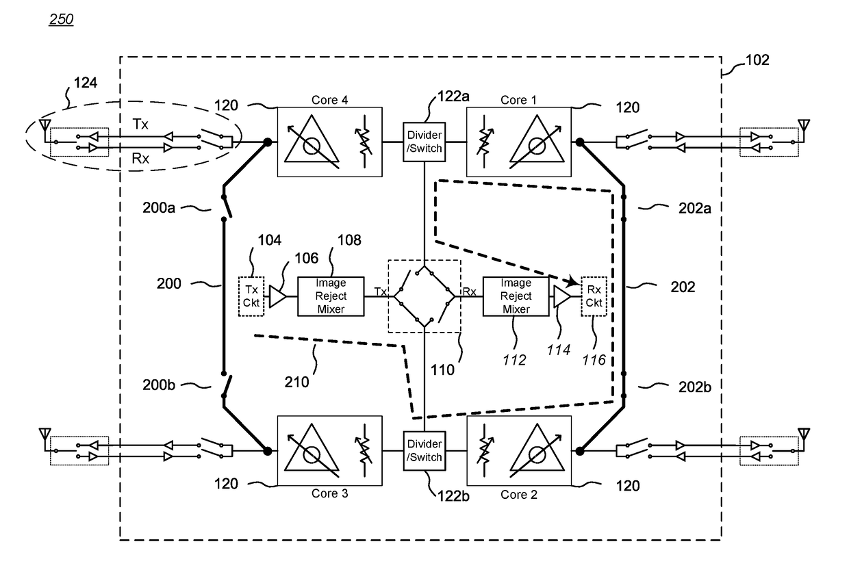
[0032]FIG. 1A is a block diagram 100 of an RF IC 102 (or “chip”) with integrated calibration circuitry suitable for use in a transceiver RF system. This particular example of an RF IC 102 is configured to be coupled to transmit circuitry 104 (labeled “Tx Ckt”) through an isolation and / or drive buffer 106 to a conventional image reject mixer 108, which in turn is coupled to a multi-way switch complex 110 (see also FIG. 1C). Also coupled to the multi-way switch complex 110 through a conventional image reject mixer 112 and an isolation and / or drive buffer 114 is receive circuitry 116 (labeled “Rx Ckt”). In alternative embodiments, conventional mixers may be used in place of the image reject mixers 108, 112. The transmit circuitry 104 and the receive circuitry 116 generally will operate at baseband frequencies, but some embodiments may operate at intermediate (IF) or RF frequencies (with appropriate adjustments in other circuitry, such as the image reject mixers 108, 112, if needed; mor...

second embodiment

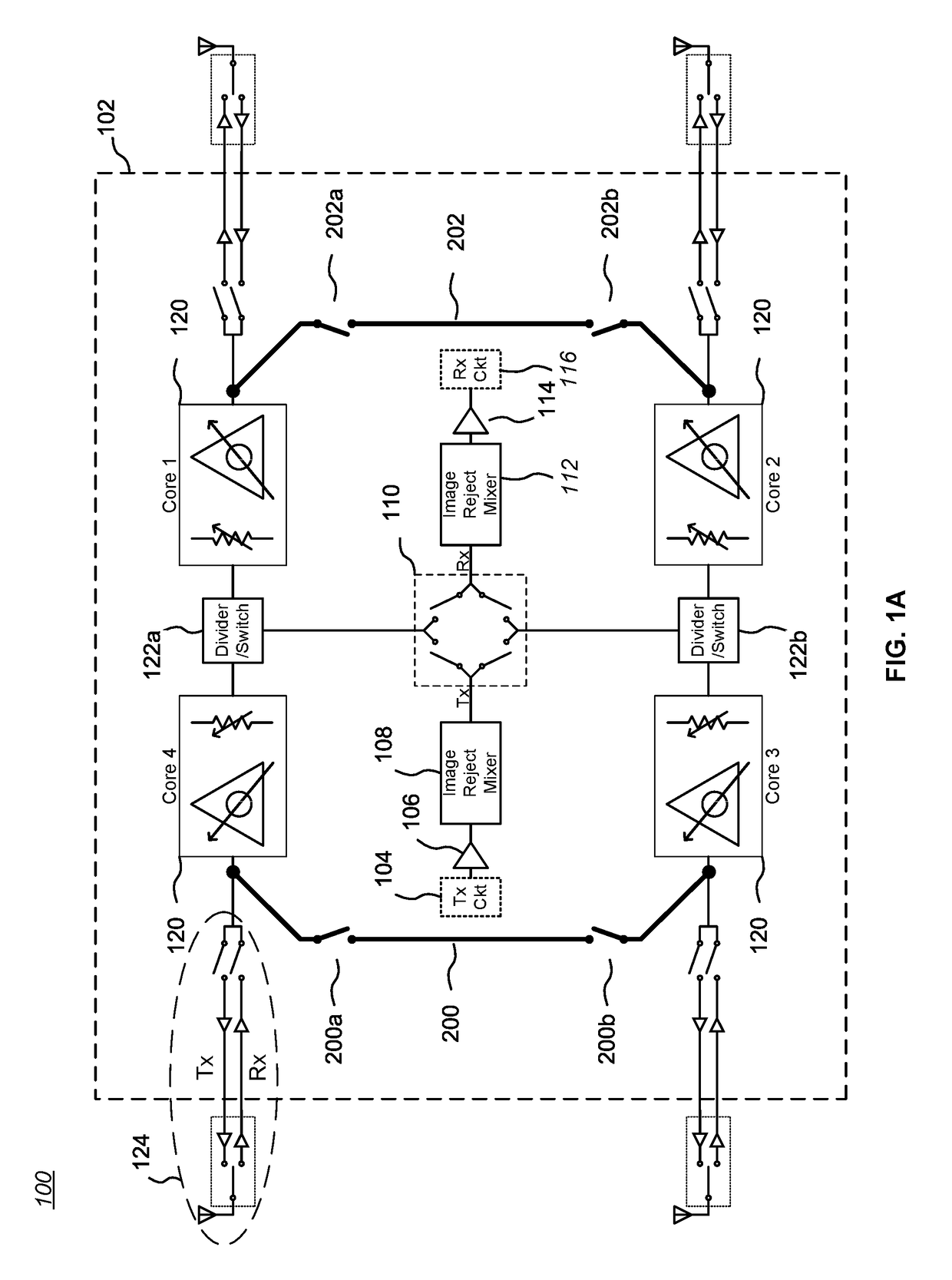
[0055]The concepts described above can be extended to include more circuitry that may affect an RF signal conveyed to or from the antennas 160. Thus, while the embodiment of FIG. 1A and FIG. 2 allows for characterization of the phase-attenuation cores 120, it is possible to extend testing to more peripheral circuitry in the RF IC 102, such as the on-chip amplifiers 154a, 156b (see FIG. 1B) in each associated input / output circuit 124. For example, FIG. 3 is a block diagram of an RF IC with integrated calibration circuitry suitable for use in a transceiver RF system. Formed on-chip with the circuit of FIG. 1A are sets of internal switchable periphery cross-circuit calibration (“PC3”) paths 302, 304, each connected to the transmit path TX and the receive path RX of pairs of phase-attenuation cores 120 by associated switches 302a-302d, 304a-304d. (Note that the PC3 paths are essentially the same as C3 paths, differing only in the connection points and number of switches, and are re-name...

third embodiment

[0072]The concepts described above can be extended to include less circuitry that may affect an RF signal conveyed to or from the antennas 160. For example, FIG. 5 is a block diagram of an RF IC with integrated calibration circuitry suitable for use in a transceiver RF system. Formed on-chip with the circuit of FIG. 1A are sets of internal switchable bypass circuit calibration (“BC2”) paths 502, 504, each connected to the reception path Rx by associated switches 502a-502b, 504a-504b. (Note that the BC2 paths are essentially the same as C3 or PC3 paths, differing only in the connection points and number of switches, and are re-named only for clarity in the following description.)

[0073]As illustrated, BC2 path 502 connects to Core 2 through switch 502a, and to Core 3 through switch 502b. Similarly, BC2 path 504 connects to Core 1 through switch 504a, and to Core 4 through switch 504b. The associated BC2 path switches may be implemented, for example, as one or more FETs or MEMS devices...


PUM


Abstract

A calibration architecture that enables accurate calibration of radio frequency (RF) integrated circuits (ICs) chips used in transceiver RF systems in a relatively simple testing environment. Embodiments of the invention include one or more on-chip switchable internal calibration paths that enable direct coupling of a portion of the on-chip circuit to an RF test system while isolating other circuitry on the chip. Some embodiments allow interconnection of switchable internal calibration paths between separate IC chips. Still other embodiments utilize internal switches and antenna mutual coupling to provide over-the-air calibration, alone or in combination with direct signal coupling via internal calibration paths. Periodic self-calibration of an RF IC can be performed after initial factory calibration, so that adjustments in desired performance parameters can be made while such an IC is embedded within a final system, and/or to take into account component degradation due to age or other factors.

Description

CROSS-REFERENCE TO RELATED APPLICATIONS[0001]This application is a continuation-in-part of and claims priority to commonly owned and co-pending U.S. patent application Ser. No. 15 / 628,524, filed Jun. 20, 2017, entitled “Integrated Circuit Calibration Architecture”, which is a continuation-in-part of and claims priority to commonly owned and co-pending U.S. patent application Ser. No. 15 / 195,379, filed Jun. 28, 2016 (now U.S. Pat. No. 9,717,008, issued Jul. 25, 2017), entitled “Integrated Circuit Calibration Architecture”, the disclosures of which are incorporated herein by reference in its entirety.BACKGROUND(1) Technical Field[0002]This invention relates to electronic circuits, and more particularly to calibration and testing architectures for radio frequency integrated circuits.(2) Background[0003]Radio frequency (RF) integrated circuits (ICs) may include a number of different RF signal paths and involve multiple inputs and outputs, such as is the case with multi-antenna / multi-tra...

Claims


Application Information

Patent Timeline
Patent Type & Authority Applications(United States)
IPC IPC(8): H04B17/14H04B17/19H04B17/13H04B1/40
CPCH04B17/14H04B17/19H04B17/13H04B1/40
Inventor SHARMA, VIKASO'LEARY, MARK JAMES
Owner PSEMI CORP
Why Eureka
Try Eureka