Check patentability & draft patents in minutes with Patsnap Eureka AI!

Retention voltage generation circuit and electronic apparatus

Active Publication Date: 2018-05-17
SEMICON MFG INT (SHANGHAI) CORP +1
View PDF1 Cites 0 Cited by
  • Summary
  • Abstract
  • Description
  • Claims
  • Application Information

AI Technical Summary

Benefits of technology

The present invention provides a circuit design for generating retention voltage to reduce power consumption and achieve data storage in wearable electronic devices. The circuit design involves generating two retention voltages using a peripheral region of memory device and selecting one with a higher voltage value as the retention voltage to drive the power-consumption circuit. This design is effective in reducing the area of the chip and achieving a low-power consumption operation status. However, the existing circuit design using a double-source voltage structure is unable to effectively reduce the area of the chip, and introduces extra time and dynamic power-consumption.

Problems solved by technology

Therefore, almost all of the manufacturers of the wearable apparatus focus on the size and the power consumption of the wearable apparatus when the wearable devices are developed.
However, when such a structure is used, the noise margin is easily reduced; and the stability of the data stored in the SRAM is affected.
Thus, the area of the IC chip cannot be further reduced.
Further, when the source voltage is switched between two statuses, it requires extra time and extra dynamic power-consumption.
However, such a circuit design is unable to effectively reduce the area of the IC chip.
On the other hand, when the double-source voltage structure is performing voltage switches, it needs extra time and extra dynamic power consumption; and the SRAM is unable to effectively achieve a low-power consumption operation status.

Method used


Image

  • Retention voltage generation circuit and electronic apparatus
  • Retention voltage generation circuit and electronic apparatus
  • Retention voltage generation circuit and electronic apparatus

Examples


Embodiment Construction

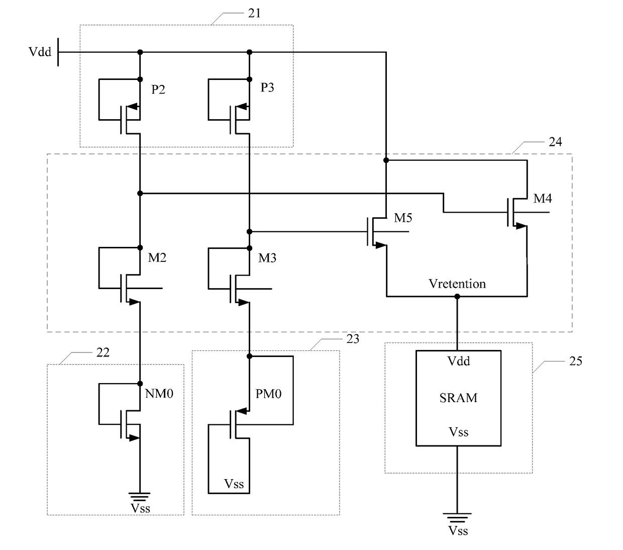
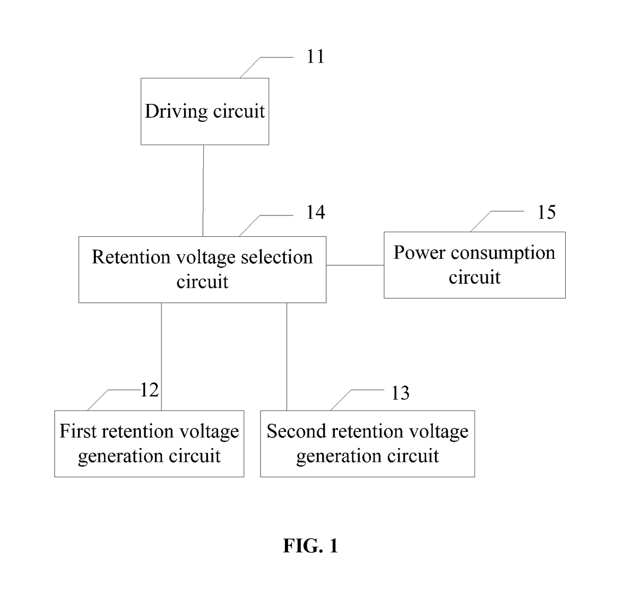
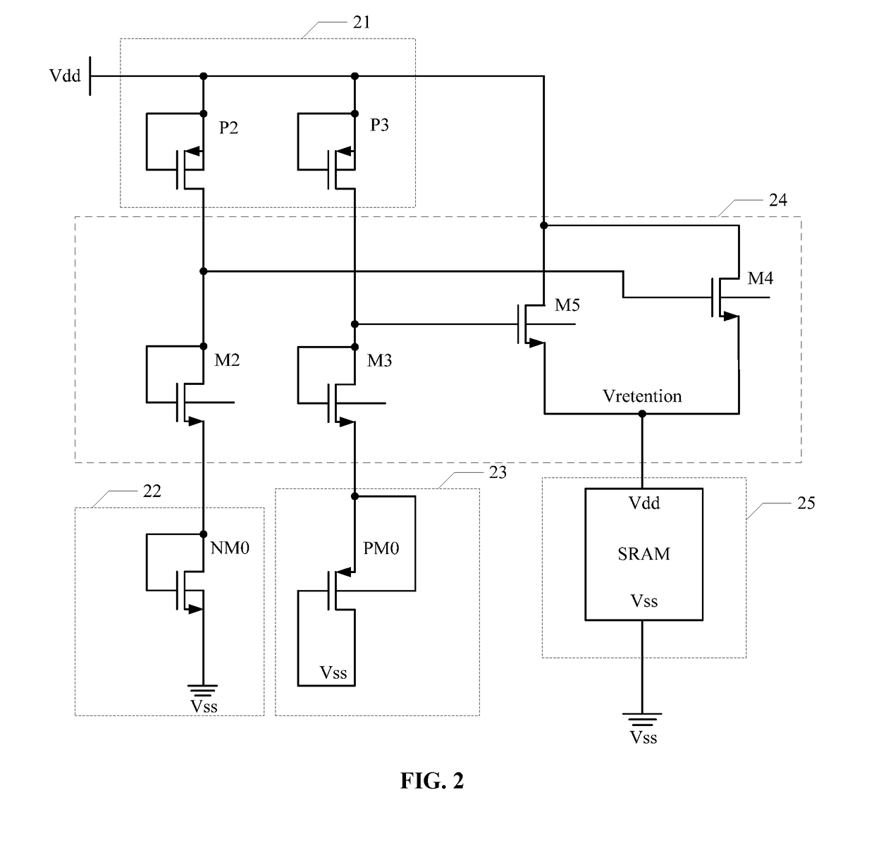
[0015]Reference will now be made in detail to exemplary embodiments of the disclosure, which are illustrated in the accompanying drawings. Wherever possible, the same reference numbers will be used throughout the drawings to refer to the same or like parts. In the description, “equal” and / or “similar” may not be limited to the strict equivalencies in the values, it may also refer to the equivalencies in an acceptable range.

[0016]Wearable electronic apparatus are often confined, due to use of a peripheral region of memory device (e.g., SRAM) to connect to an external double-source voltage structure to generate retention voltage, so as to reduce the power consumption of the electronic apparatus and to achieve a data storage function simultaneously. However, such a circuit design is unable to effectively reduce the area of the chip. On the other hand, when externally connected double-source voltage structure is switching the voltages, it is easy to introduce extra time and dynamic powe...


PUM


Abstract

Retention voltage generation circuits and electronic apparatus are provided. An exemplary retention voltage generation circuit includes a driving circuit, configured to generate driving currents; a first retention voltage generation circuit, configured to generate a first retention voltage, the first retention voltage being substantially equal to a threshold voltage of an NMOS transistor in a power-consumption circuit; a second retention voltage generation circuit, configured to generate a second retention voltage, the second retention voltage being substantially equal to a threshold voltage of a PMOS transistor in the power-consumption circuit; and a retention voltage selection circuit, coupled to the first retention voltage generation circuit and the second retention voltage generation circuit, and configured to receive the driving currents, wherein retention voltage selection circuit is configured to select a higher voltage from the first retention voltage and the second retention voltage as a retention voltage to drive the power-consumption circuit to operate at a retention mode.

Description

CROSS-REFERENCES TO RELATED APPLICATIONS[0001]This application claims the priority of Chinese patent application No. 201610994781.X, filed on Nov. 11, 2016, the entirety of which is incorporated herein by reference.FIELD OF THE DISCLOSURE[0002]The present disclosure generally relates to the field of integrated circuits (ICs) and, more particularly, relates to retention voltage generation circuits and electronic apparatus.BACKGROUND[0003]With the continuous development of intelligent wearable technologies, more and more wearable apparatus have penetrated into every part of people's daily life. The intelligent wearable apparatus includes intelligent watches, and heath wristbands, etc. For the development of the wearable apparatus, the size and the power consumption are the two key factors to evaluate if a wearable apparatus is able to attract customers' attentions. For the intensively competitive market of the wearable apparatus, weather the wearable apparatus are able to attract the ...

Claims


Application Information

Patent Timeline
IPC IPC(8): G11C11/412G11C11/417
CPCG11C11/4125G11C11/417G05F1/561G05F3/24G11C5/14G11C5/143H02J4/00
Inventor SZETO, SIMON TO-MINGWU, LEI
Owner SEMICON MFG INT (SHANGHAI) CORP
Features
  • R&D
  • Intellectual Property
  • Life Sciences
  • Materials
  • Tech Scout
  • Unparalleled Data Quality
  • Higher Quality Content
  • 60% Fewer Hallucinations
Learn More