Mass Transfer Of Micro Structures Using Adhesives

a micro-structure and adhesive technology, applied in the direction of semiconductor/solid-state device manufacturing, semiconductor/semiconductor devices, electrical equipment, etc., can solve the problems of limited battery operation time, low light efficiency, and high power consumption

Active Publication Date: 2018-06-14
JADE BIRD DISPLAY SHANG HAI LTD
View PDF4 Cites 72 Cited by
  • Summary
  • Abstract
  • Description
  • Claims
  • Application Information

AI Technical Summary

Problems solved by technology

However, conventional LCD displays suffer from low light efficiency, causing high power consumption and limited battery operation time.
However, the integration of thousands or even millions of micro LEDs with a pixel driver circuit array is quite challenging.
However, this fabrication process is inefficient and costly.
The substrate on which the micro LEDs is fabricated remains in the final product, which may cause light cross-talk.
Additionally, the thermal mismatch between the two different substrates generates stress at the bonding interface, which can cause reliability issues.
Furthermore, multi-color display panels typically require more micro LEDs and different color micro LEDs grown on different substrate materials, compared with single-color display panels, thus making the traditional manufacturing process even more complicated and inefficient.
For example, they may have different thermal coefficients of expansion which make it difficult to bond the micro LEDs to the pixel driver circuitry while both are still on their original substrates.

Method used


Image

  • Mass Transfer Of Micro Structures Using Adhesives
  • Mass Transfer Of Micro Structures Using Adhesives
  • Mass Transfer Of Micro Structures Using Adhesives

Examples


Embodiment Construction

[0024]The figures and the following description relate to preferred embodiments by way of illustration only. It should be noted that from the following discussion, alternative embodiments of the structures and methods disclosed herein will be readily recognized as viable alternatives that may be employed without departing from the principles of what is claimed.

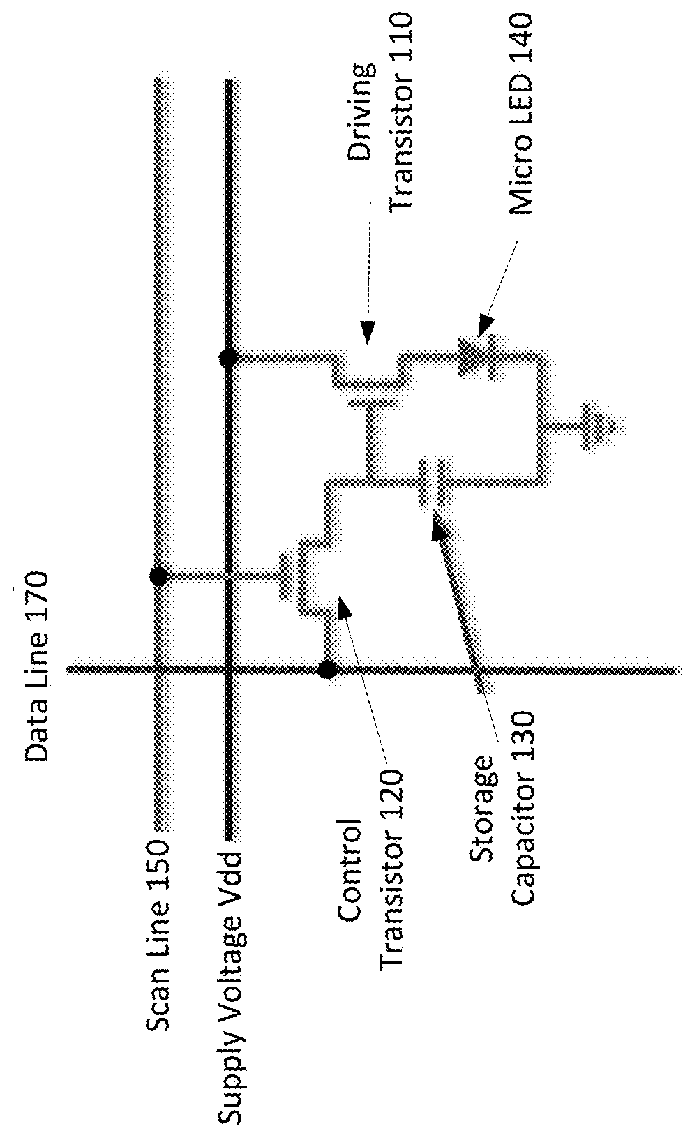
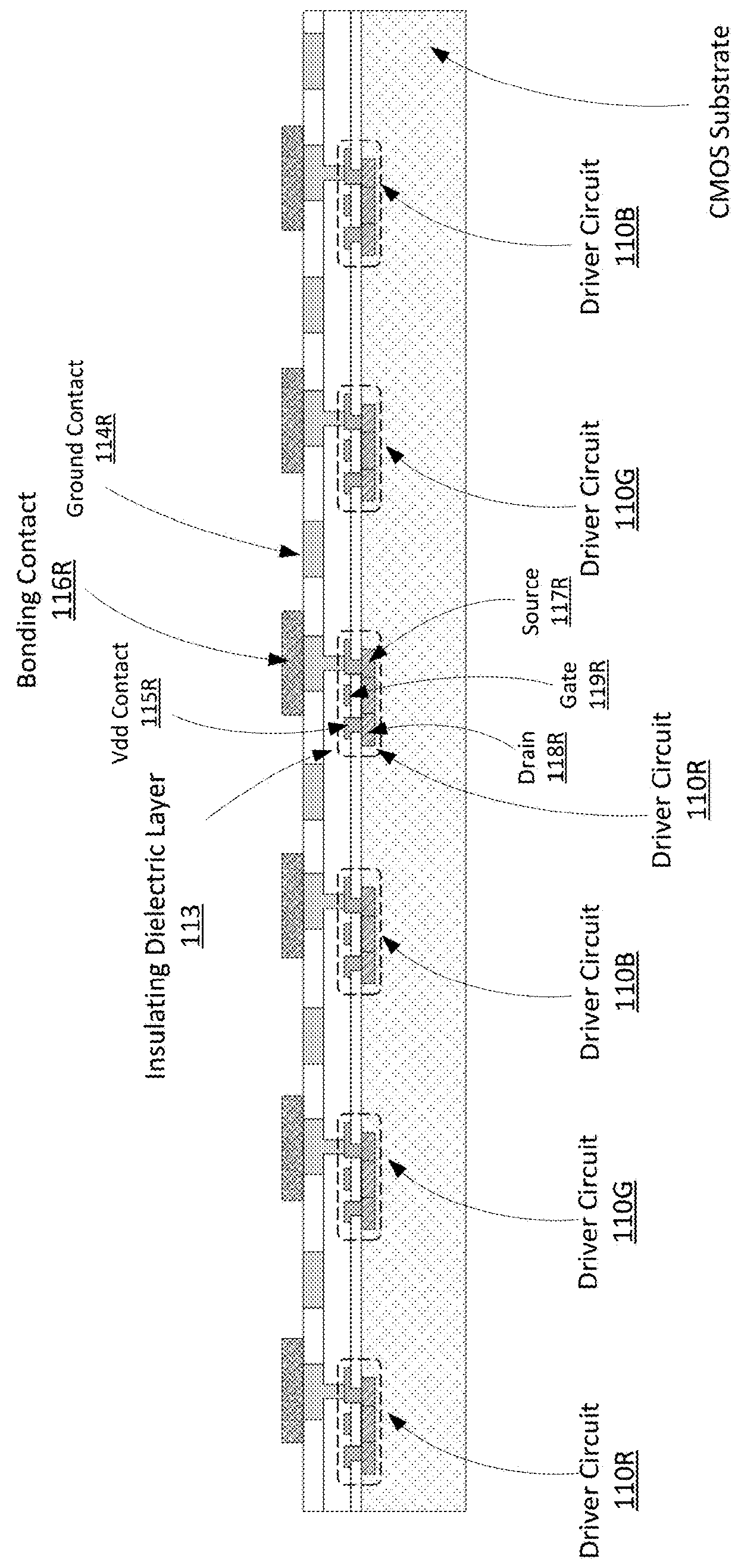
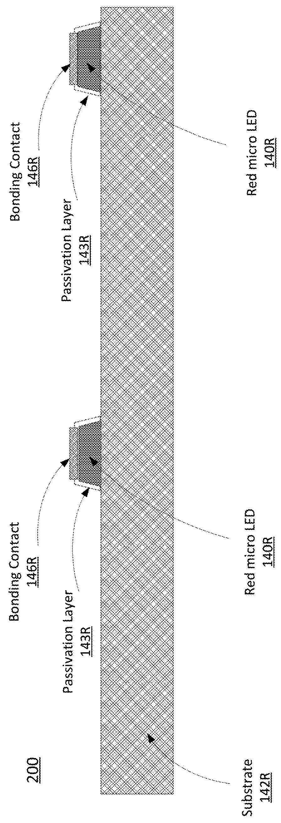
[0025]The following examples primarily use an integrated micro LED display in which array(s) of GaN micro LEDs are attached to CMOS pixel drivers by eutectic bonding, but these are just examples and the techniques described are not limited to this particular application. Examples of micro LEDs include GaN based UV / blue / green micro LEDs, AlInGaP based red / orange micro LEDs, and GaAs or InP based infrared (IR) micro LEDs. Additional examples of micro LEDs and other micro structures are described in U.S. patent application Ser. No. 15 / 135,217 “Semiconductor Devices with Integrated Thin-Film Transistor Circuitry”, Ser. No. 15 / 269,...


PUM


Abstract

Mass transfer of micro structures are effected from one substrate to another using adhesives. In the context of an integrated micro LED display, a micro LED array is fabricated on a native substrate and corresponding CMOS pixel drivers are fabricated on a separate substrate. The micro LED substrate (e.g., sapphire) and the CMOS substrate (e.g., silicon) may be incompatible. For example, they may have different thermal coefficients of expansion which make it difficult to bond the micro LEDs to the pixel driver circuitry. The micro LED array is transferred to an intermediate substrate (e.g., silicon) by use of an adhesive. This intermediate substrate may be used in a process of bonding the micro LED array to the array of pixel drivers. The intermediate substrate is separated from the micro LED array by releasing the adhesive.

Description

CROSS-REFERENCE TO RELATED APPLICATION(S)[0001]This application claims priority under 35 U.S.C. § 119(e) to U.S. Provisional Patent Application Ser. No. 62 / 433,741, “Mass Transfer of Micro Structures using Adhesives,” filed Dec. 13, 2016. The subject matter of all of the foregoing is incorporated herein by reference in their entirety.BACKGROUND1. Technical Field[0002]This disclosure relates generally to methods for fabricating semiconductor devices, including integrated multi-color micro LED display panels.2. Description of Related Art[0003]Active matrix liquid-crystal displays (LCD) and organic light emitting diode (OLED) displays combined with thin-film transistor (TFT) technology are becoming increasingly popular in today's commercial electronic devices. These displays are widely used in laptop personal computers, smartphones and personal digital assistants. Millions of pixels together create an image on a display. The TFTs act as switches to individually turn each pixel on and o...

Claims


Application Information

Patent Timeline
Patent Type & Authority Applications(United States)
IPC IPC(8): H01L25/16H01L33/62H01L33/00
CPCH01L25/167H01L33/62H01L33/0079H01L2933/0066H01L27/124H01L27/1255H01L33/32H01L25/0753H01L21/6835H01L2221/68354H01L2221/68368H01L33/0093H01L24/89H01L24/94H01L27/156H01L33/0095H01L21/30604H01L21/31116H01L21/324H01L27/15H01L33/00H01L33/08
Inventor CHONG, WING CHEUNGZHANG, LEIOU, FANGLI, QIMING
Owner JADE BIRD DISPLAY SHANG HAI LTD
Why Eureka
Try Eureka