
Method for making gallium nitride epitaxial layer by silicon substrate

Active Publication Date: 2018-07-12
TSINGHUA UNIV +1
View PDF0 Cites 0 Cited by
  • Summary
  • Abstract
  • Description
  • Claims
  • Application Information

AI Technical Summary

Benefits of technology

The patent is about a way to make a layer of gallium nitride (GaN) on a silicon substrate. The technical effect of this method is the ability to create high-quality GaN layers on silicon, which can be useful in a variety of applications.

Problems solved by technology

The use of sapphire substrate is problematic due to lattice mismatch and thermal expansion mismatch between GaN and the sapphire substrate.
One consequence of thermal expansion mismatch is bowing of the GaN / sapphire substrate structure, which leads to cracking and difficulty in fabricating devices with small feature sizes.
However, the process of lithography is complex, high in cost, and will pollute the sapphire substrate, specifically, the GaN epitaxial layer grown on the sapphire substrate is more preferred over the GaN epitaxial layer grown on the silicon substrate.

Method used


Image

  • Method for making gallium nitride epitaxial layer by silicon substrate
  • Method for making gallium nitride epitaxial layer by silicon substrate
  • Method for making gallium nitride epitaxial layer by silicon substrate

Examples


Embodiment Construction

[0034]It will be appreciated that for simplicity and clarity of illustration, where appropriate, reference numerals have been repeated among the different figures to indicate corresponding or analogous elements. In addition, numerous specific details are set forth in order to provide a thorough understanding of the exemplary embodiments described herein. However, it will be understood by those of ordinary skill in the art that the exemplary embodiments described herein can be practiced without these specific details. In other instances, methods, procedures, and components have not been described in detail so as not to obscure the related relevant feature being described. The drawings are not necessarily to scale, and the proportions of certain portions may be exaggerated better illustrate details and features. The description is not to considered as limiting the scope of the exemplary embodiments described herein.

[0035]Several definitions that apply throughout this disclosure will n...


PUM


Abstract

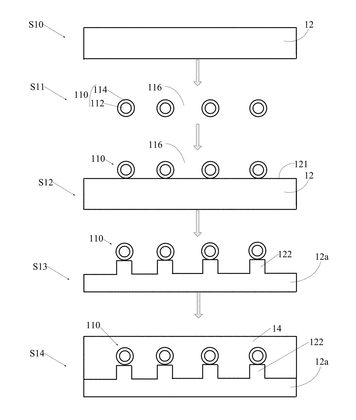
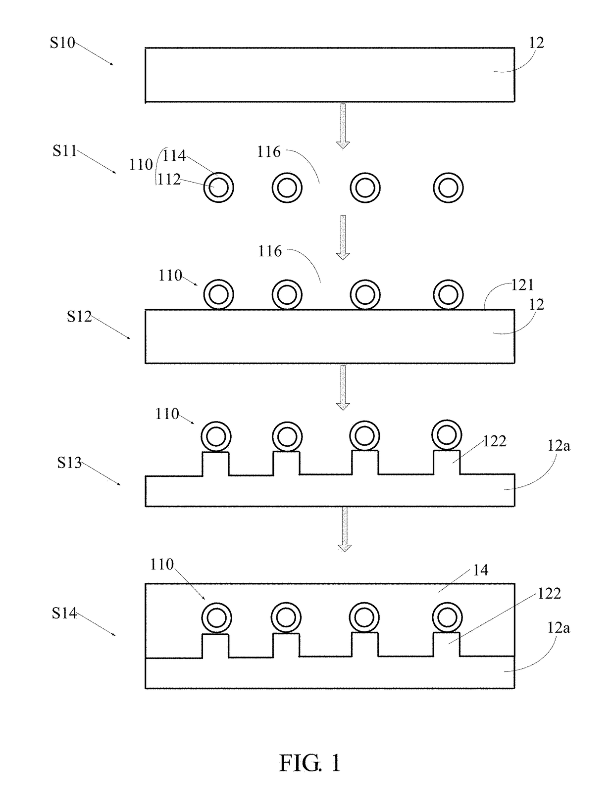
The disclosure relates to a method for making gallium nitride (GaN) epitaxial layer by silicon substrate is related. The method includes: providing a silicon substrate; providing a carbon nanotube structure comprising a plurality of carbon nanotubes and defining a plurality of holes; forming the carbon nanotube structure on a surface of the silicon substrate so that portions of the silicon substrate are exposed; dry etching the silicon substrate using the carbon nanotube structure as mask to obtain a patterned silicon substrate having a pattern surface comprising a plurality of bulges; and growing the GaN epitaxial layer using the patterned silicon substrate as an epitaxial substrate.

Description

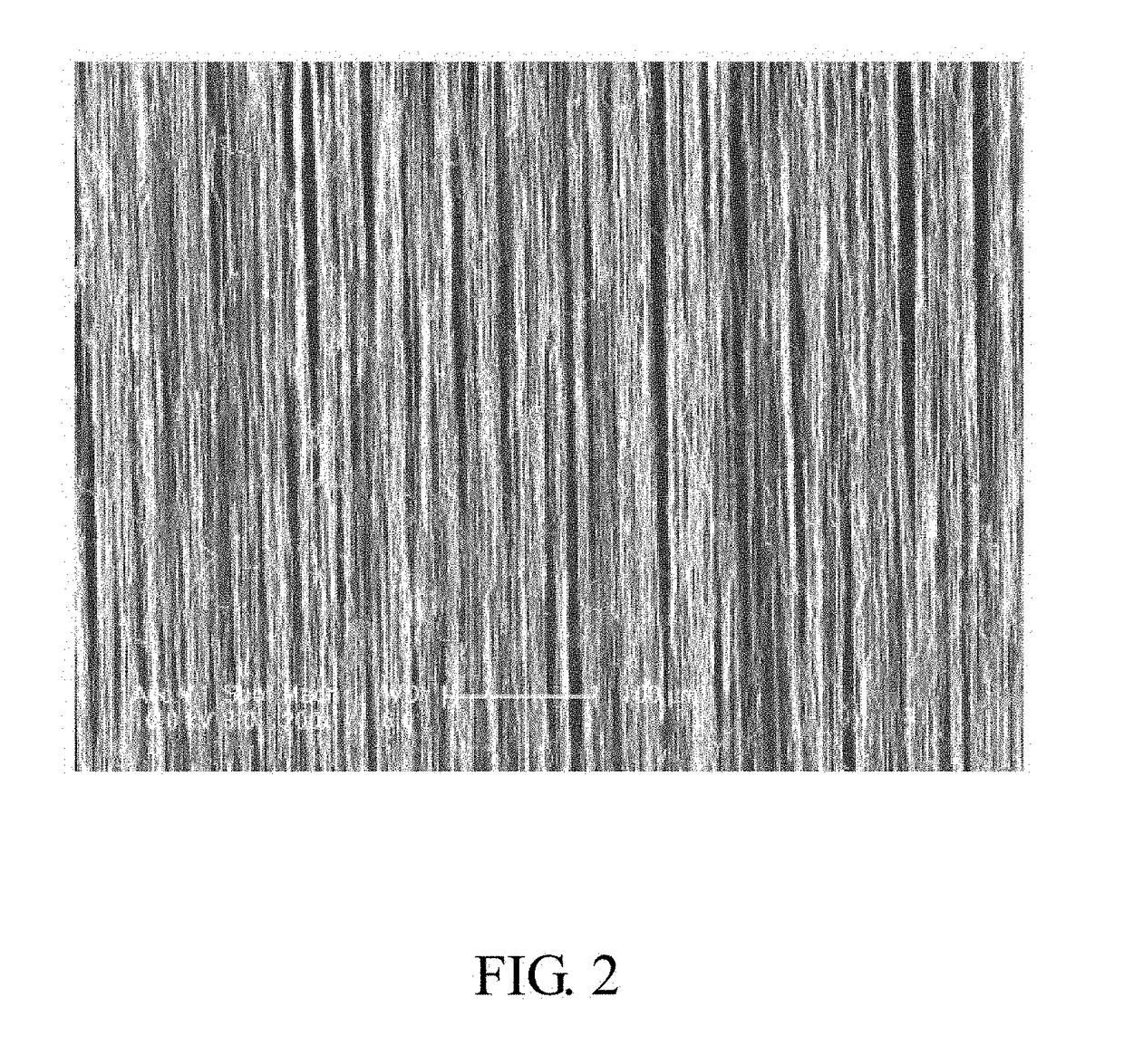
CROSS-REFERENCE TO RELATED APPLICATIONS[0001]This application claims all benefits accruing under 35 U.S.C. § 119 from China Patent Application No. 201710017094.7, filed on Jan. 10, 2017, in the China Intellectual Property Office, the disclosure of which is incorporated herein by reference.BACKGROUND1. Technical Field[0002]The present disclosure relates to a method for making gallium nitride (GaN) epitaxial layer by silicon substrate.2. Description of Related Art[0003]Light emitting devices such as light emitting diodes (LEDs) based on group III-V nitride semiconductors (e.g. GaN) have been put into practice.[0004]Since wide GaN substrate cannot be produced, the LEDs have been produced on a heteroepitaxial substrate such as sapphire. The use of sapphire substrate is problematic due to lattice mismatch and thermal expansion mismatch between GaN and the sapphire substrate. One consequence of thermal expansion mismatch is bowing of the GaN / sapphire substrate structure, which leads to cr...

Claims


Application Information

Patent Timeline
IPC IPC(8): C30B25/18H01L21/02C30B29/40
CPCC30B25/186H01L21/0254H01L21/02381H01L21/02444H01L21/02642C30B29/406H01L21/0243H01L21/02617H01L33/007H01L33/20H01L33/32H01L21/0262H01L21/02639H01L21/0265H01L21/02658
Inventor JIN, YUAN-HAOLI, QUN-QINGFAN, SHOU-SHAN
Owner TSINGHUA UNIV
Learn More