Supercharge Your Innovation With Domain-Expert AI Agents!

Semiconductor light emitting device and method of manufacturing the same

a technology of semiconductor light and light emitting device, which is applied in the direction of semiconductor/solid-state device manufacturing, semiconductor devices, and electrical equipment, etc., can solve the problems of reducing the life of the device, unable to completely extract light, and unable to discharge light from the semiconductor light emitting devi

Active Publication Date: 2018-07-12
SAMSUNG ELECTRONICS CO LTD
View PDF0 Cites 0 Cited by
  • Summary
  • Abstract
  • Description
  • Claims
  • Application Information

AI Technical Summary

Benefits of technology

The patent describes a semiconductor light emitting device with improved adhesion between the layers. The device includes a light emitting structure, an insulating layer with two openings, an electrode layer with two electrodes, and an adhesive layer with two openings. The adhesive layer overlaps the insulating layer and the electrode layer, providing better stability and reduced risk of delamination. The device also includes a method of manufacturing the device with the adhesive layer that provides improved adhesion between the layers. This design and method improve the reliability and efficiency of semiconductor light emitting devices.

Problems solved by technology

Further, light which fails to be discharged from the semiconductor light emitting device generates heat while moving internally.
The generated heat may decrease the life of the device.
However, during a process, light generated in an active layer may be affected by a refractive index of each layer such that the light fails to be totally extracted.

Method used


Image

  • Semiconductor light emitting device and method of manufacturing the same
  • Semiconductor light emitting device and method of manufacturing the same
  • Semiconductor light emitting device and method of manufacturing the same

Examples


Embodiment Construction

[0017]Exemplary embodiments of the inventive concept will now be described in detail with reference to the accompanying drawings.

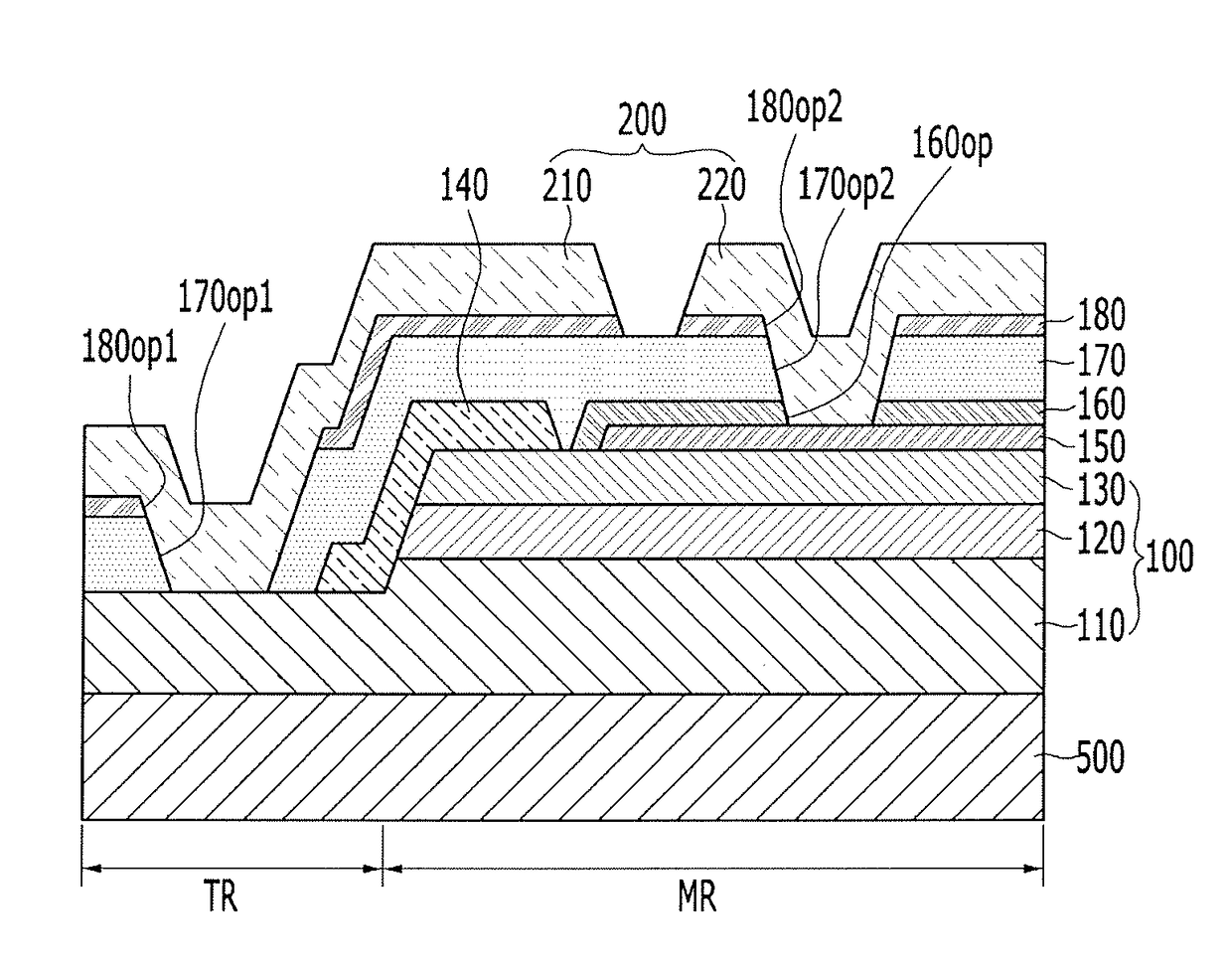
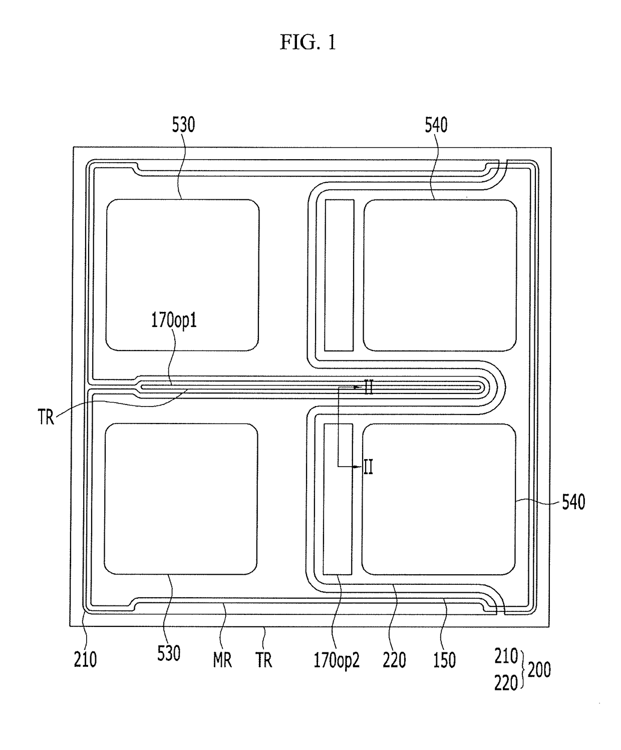
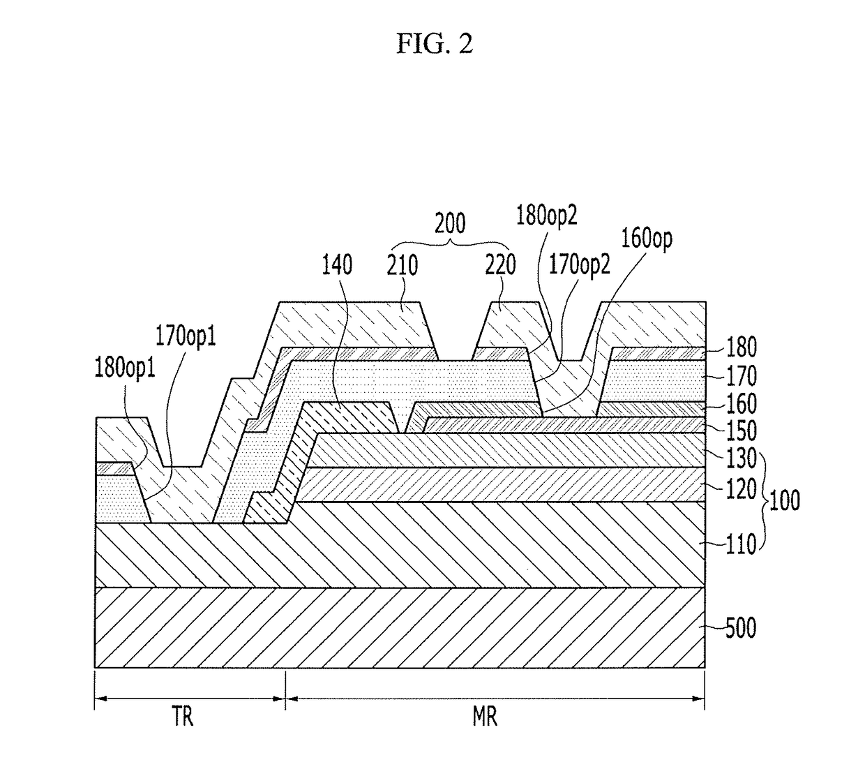
[0018]FIG. 1 is a top plan view illustrating a semiconductor light emitting device according to an exemplary embodiment of the inventive concept. FIG. 2 is a cross-sectional view, taken along line II-II of FIG. 1, illustrating the semiconductor light emitting device of FIG. 1, according to an exemplary embodiment of the inventive concept.

[0019]Referring to FIGS. 1 and 2, a semiconductor light emitting device includes a substrate 500 and a light emitting structure 100 formed on the substrate 500. The light emitting structure 100 may include a first conductive semiconductor layer 110, an active layer 120 disposed on the first conductive semiconductor layer 110, and a second conductive semiconductor layer 130 disposed on the active layer 120.

[0020]The substrate 500 may be a transparent substrate. For example, the substrate 500 may include sapphire (Al2O3), ga...


PUM


Abstract

A semiconductor light emitting device includes a light emitting structure in which a first conductive semiconductor layer, an active layer, and a second conductive semiconductor layer are sequentially laminated, an insulating layer disposed on the light emitting structure and including first and second openings, an electrode layer disposed on the insulating layer and including first and second electrodes, and an adhesive layer disposed between the electrode layer and the insulating layer and including first and second openings. The first opening of the adhesive layer overlaps the first opening of the insulating layer and is equal to or larger than the first opening of the insulating layer. The second opening of the adhesive layer overlaps the second opening of the insulating layer and is equal to or larger than the second opening of the insulating layer.

Description

CROSS-REFERENCE TO RELATED APPLICATION[0001]This application claims priority under 35 U.S.C. § 119 to Korean Patent Application No. 10-2017-0003578, filed in the Korean Intellectual Property Office on Jan. 10, 2017, the disclosure of which is incorporated by reference herein in its entirety.TECHNICAL FIELD[0002]The inventive concept relates to a light emitting device, and more particularly, to a semiconductor light emitting device and a method of manufacturing the same.DISCUSSION OF THE RELATED ART[0003]A semiconductor light emitting device is a semiconductor device capable of generating light by recombination of electrons and holes in a junction portion of p-type and n-type semiconductors when a current is applied. The semiconductor light emitting device has various attractive features such as a relatively long life, low power consumption, good initial driving characteristics, and a high vibration resistance when compared to an incandescent light emitting device. Thus, demand for s...

Claims


Application Information

Patent Timeline
IPC IPC(8): H01L33/22H01L21/02H01L33/00H01L33/38
CPCH01L33/22H01L21/0237H01L21/0243H01L21/02521H01L21/02458H01L2224/05001H01L21/02502H01L33/007H01L33/38H01L2933/0016H01L33/42H01L21/02488H01L24/03H01L24/05H01L24/13H01L24/16H01L2224/0401H01L2224/13101H01L2224/16245H01L33/486H01L33/60H01L2924/014H01L2924/00014H01L33/02H01L33/0008H01L33/36H01L33/005H01L2933/0033H01L2924/12041
Inventor SIM, JAE INYOON, JU HEONKIM, GI BUMLEE
Owner SAMSUNG ELECTRONICS CO LTD
Features
  • R&D
  • Intellectual Property
  • Life Sciences
  • Materials
  • Tech Scout
  • Unparalleled Data Quality
  • Higher Quality Content
  • 60% Fewer Hallucinations
Learn More