Clock and data recovery circuit with jitter tolerance enhancement

a clock and data recovery circuit technology, applied in the field of clock and data recovery circuits, can solve the problems of significant bandwidth change, affecting the performance of the clock and data recovery circuit, and the bandwidth of the loop, so as to achieve the effect of increasing jitter toleran

Active Publication Date: 2018-07-12
NOVATEK MICROELECTRONICS CORP
View PDF8 Cites 11 Cited by
  • Summary
  • Abstract
  • Description
  • Claims
  • Application Information

AI Technical Summary

Benefits of technology

[0005]The disclosure provides a circuit to detect a loop bandwidth variation of a clock and data recovery (CDR) circuit, and adjust a loop bandwidth of the CDR circuit by adjusting proportional path and integral path gain factors of a digital filter of the CDR circuit. Accordingly, the CDR circuit is able to maintain a proper loop bandwidth and increase jitter tolerance.
[0006]The CDR circuit of the present disclosure provides jitter tolerance enhancement in the CDR circuit, which includes: a bang-bang phase detector (BBPD), a digital filter, a digitally controlled oscillator (DCO), and an adaptive loop gain control (ALGC) circuit. The ALGC circuit generates the information for adjusting the loop bandwidth of the CDR circuit according to the phase difference information signal from BBPD. The loop bandwidth of the CDR circuit is adjusted by adjusting gain factors in the loop gain of the CDR circuit. For adjusting the loop bandwidth of the CDR circuit, two possible methods are alternatively adopted by the ALGC circuit, including: a bang-bang adjusting method, and a linear adjusting method. Thereby, the CDR circuit may have a better jitter tolerance.

Problems solved by technology

However, use of the bang-bang phase detector for generating phase difference information leads to two issues, one is the bang-bang phase detector may have different gain due to varying jitter in the input data, which cause loop bandwidth to vary frequently, and the other issue is the input data having a high transition density may results in significant change in bandwidth, thus affecting the performance of the CDR circuit.

Method used


Image

  • Clock and data recovery circuit with jitter tolerance enhancement
  • Clock and data recovery circuit with jitter tolerance enhancement
  • Clock and data recovery circuit with jitter tolerance enhancement

Examples


Embodiment Construction

[0020]A term “couple” used in the full text of the disclosure (including the claims) refers to any direct and indirect connections. For an instance, if a first circuit is described to be coupled to a second circuit, it is interpreted as that the first circuit is directly coupled to the second circuit, or the first circuit is indirectly coupled to the second circuit through other circuit or connection means. Moreover, wherever possible, components / members / steps using the same referential numbers in the drawings and description refer to the same or like parts. Components / members / steps using the same referential numbers or using the same terms in different embodiments may cross-refer to related descriptions.

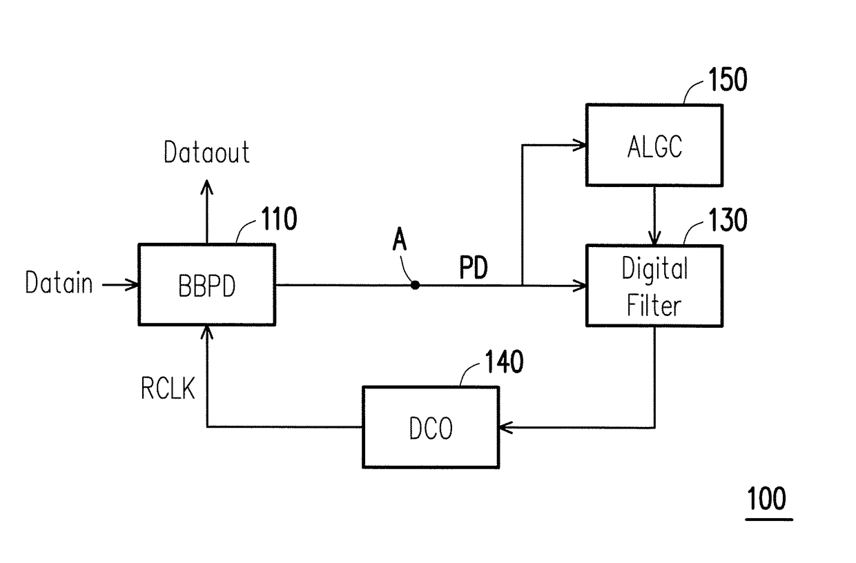
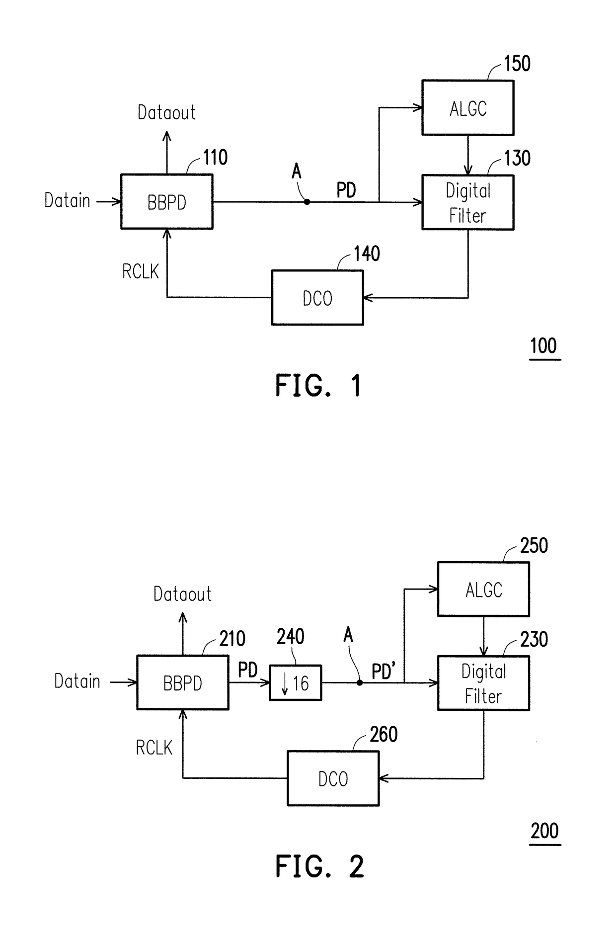
[0021]FIG. 1 is a schematic block diagram of a clock and data recovery (CDR) circuit 100 according to an exemplary embodiment of the disclosure. As shown in FIG. 1, the CDR circuit 100 includes a bang-bang phase detector (BBPD) 110, a digital filter 130, a digitally controlled oscil...


PUM


Abstract

A clock and data recovery circuit with jitter tolerance enhancement is provided. The CDR circuit includes: a bang-bang phase detector, a digital filter, a digitally controlled oscillator, and an adaptive loop gain control circuit. The CDR circuit detects a loop bandwidth variation and adjusts the loop bandwidth of CDR circuit by adjusting proportional path and integral path gain factors of the digital filter of the CDR circuit. The loop gain controller uses two methods to adjust the loop gain in CDR circuit: bang-bang adjusting method and linear adjusting method.

Description

CROSS-REFERENCE TO RELATED APPLICATION[0001]This application claims the priority benefit of U.S. provisional application Ser. No. 62 / 442,994, filed on Jan. 6, 2017. The entirety of the above-mentioned patent application is hereby incorporated by reference herein and made a part of this specification.BACKGROUNDTechnical Field[0002]The present disclosure relates to a clock and data recovery circuit, and more particularly, to a clock and data recovery circuit with jitter tolerance enhancement by detecting variation in the loop bandwidth thereby adjusting the loop bandwidth.Description of Related Art[0003]A receiver of a high-speed transmission system often has to perform an appropriate recovery processing to the input data signal to detect an embedded clock signal by using a clock and data recovery (CDR) circuit. A conventional CDR circuit includes a bang-bang phase detector (BBPD), a loop filter and an oscillator. In terms of operation, the oscillator may generate a sampling clock sig...

Claims


Application Information

Patent Timeline
Patent Type & Authority Applications(United States)
IPC IPC(8): H04L7/00H03L7/08H03L7/089H03L7/093H03L7/091
CPCH04L7/0016H03L7/0807H03L7/0891H03L7/093H03L7/091H03L7/0992H03L7/113H03L7/18H03L7/087H03L7/0898H03L2207/06H04L7/0331
Inventor HUANG, CHANG-CHENGLIU, SHEN-IUANHUANG, JU-LINTZENG, TZU-CHIENLIANG, KEKO-CHUNWANG, YU-HSIANGYEH, CHE-WEI
Owner NOVATEK MICROELECTRONICS CORP
Why Eureka
Try Eureka