Image processing method and display device

a technology of image processing and display device, which is applied in the field of image processing technique, can solve the problems of image sticking, reduced emitting efficiency, and reduced life cycle of display panel, and achieve the effects of reducing the luminance reducing the decay speed and prolonging the life of light emitting elements

Active Publication Date: 2018-07-19
NOVATEK MICROELECTRONICS CORP
View PDF0 Cites 3 Cited by
  • Summary
  • Abstract
  • Description
  • Claims
  • Application Information

AI Technical Summary

Benefits of technology

[0005]The invention provides an image processing method and a display device capable of gradually reducing luminance of light emitting elements (e.g., OLED elements) by a plurality of image proces

Problems solved by technology

As an OLED element is used for a long time, or driven by high luminance, material deterioration occurs to the OLED element, which leads to reduced emitting efficiency, decreased life cycle of a display panel, and occurrence of defects, such as image sticking, on the display panel.
Additionally, recent displays tends to be provided with high resolution to present delicate images.
As a result, a light-emitting area of the OLED element for presenting each pixel is gradually reduced, such that

Method used


Image

  • Image processing method and display device
  • Image processing method and display device
  • Image processing method and display device

Examples


first embodiment

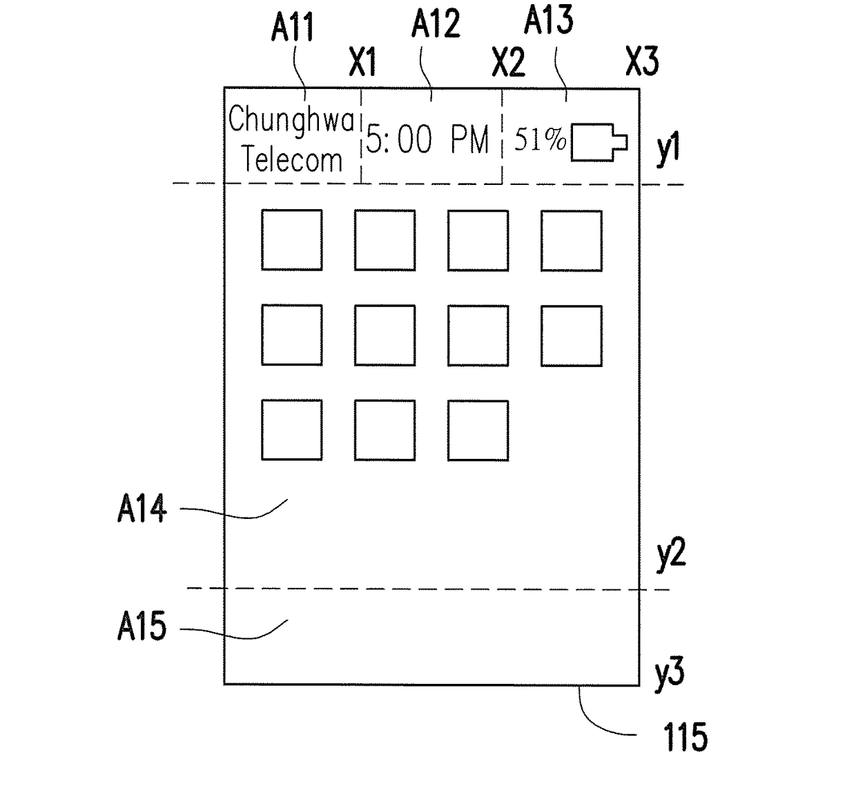
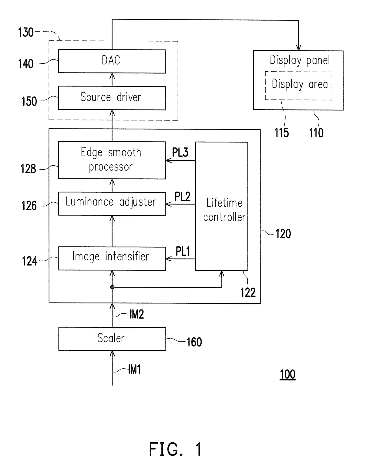
[0022]FIG. 1 is a functional block diagram of a display device 100 according to the invention. The display device 100 is a consumer electronic device, such as a cell phone, a tablet computer and a notebook computer, or a home appliance provided with a display screen, such as a television. Referring to FIG. 1, the display device 100 includes a display panel 110, a panel driver 130 and a display controller 120. In the present embodiment, the panel driver 130 may include a digital-to-analog converter (DAC) 140 and a source driver 150. In some of the embodiments, the panel driver 130 may also include a timing controller, or the function of the timing controller may be integrated in the display controller 120 of the display apparatus 100. The display panel 100 may be composed of a solid state light source, for example, a light-emitting diode (LED) element or an organic light emitting diode (OLED) element. The display panel 110 may be a non-flexible display panel or a flexible display pan...

second embodiment

[0044]Besides being determined to degrade the processing level corresponding to the image processing scheme according to the duration in which the image is maintained still, the processing level may also be determined to degrade according to a bending degree of the display area, so as to reduce the luminance of the image in a scenario that the display panel is a flexible display panel. FIG. 10 is a functional block diagram of a display device 1000 according to the invention. Referring to FIG. 10, the display device 1000 includes a display panel 1010, a panel driver 1030, a display controller 1020 and a bending detector 1060. The panel driver 1030 is configured to drive the display panel 1010. The display controller 1020 is coupled to the panel driver 1030 and the bending detector 1060. The panel driver 1030 may include a DAC 1040 and a source driver 1050. The display panel 1010 may be composed of a solid state light source, for example, an organic light emitting diode (OLED) element...


PUM


Abstract

An image processing method and a display device thereof are provided. The method is adapted to a display panel with a display area. The image processing method includes the following steps. Whether original images to be displayed on a plurality of sub-areas of the display area are still is analyzed and determined. When the original image in a current sub-area is still, a time length of the original image being still is recorded. The current sub-area is one of the sub-areas. Processing levels corresponding to a plurality of image processing schemes are determined based on the time length. Overall or partial luminance (luma) of the original image in the current sub-area is gradually reduced by the image processing schemes with the determined processing levels, and a corresponding luma-reduced image is displayed on the current sub-area.

Description

BACKGROUNDField of the Invention[0001]The invention is directed to an image processing technique and more particularly, an image processing method and a display device thereof capable of extending a lifetime of a display panel.Description of Related Art[0002]A solid state light source (e.g., a light-emitting diode (LED), an organic light-emitting diode (OLED), etc.), in comparison with a fluorescent lamp or an incandescent lamp of the related art, has advantages, such as small volume, long lifetime, high reliability and so on, thus, has become the focus of development of the optoelectronic industry and widely applied in the lighting market and display devices in a variety of sizes. The OLED is self-luminous and does not need any backlight source, such that an OLED film has a thin characteristic to achieve light transparency and a better development vision than the LED.[0003]As an OLED element is used for a long time, or driven by high luminance, material deterioration occurs to the ...

Claims


Application Information

Patent Timeline
IPC IPC(8): G09G3/20
CPCG09G3/2003G09G2320/0626G09G2320/0666G09G2320/046G09G2320/048G09G2320/103G09G2360/16G09G3/3208G09G5/10G06F1/1652G09G3/035G06F1/1677G06T5/002G06T2207/20024G09G2320/045
Inventor YANG, HSUEH-YENCHANG, HUA-GANGLIN, CHUN-CHIEH
Owner NOVATEK MICROELECTRONICS CORP
Why Eureka
Try Eureka