Inductor device

a technology of a conductor and a spherical plate, which is applied in the direction of transformer/inductance details, printed inductances, inductances, etc., can solve the problem of easy electrical shortening of the conductor pattern layer, and achieve the effect of increasing the cross-sectional area of the first base conductor layer

Active Publication Date: 2018-08-02
SHINKO ELECTRIC IND CO LTD
View PDF4 Cites 11 Cited by
  • Summary
  • Abstract
  • Description
  • Claims
  • Application Information

AI Technical Summary

Benefits of technology

[0037]For this reason, it is possible to increase the cross-sectional area of the first bas

Problems solved by technology

In the method of forming the conductor pattern layer, when a pitch of the base copper layer pattern is narrowed, the adjacent secon

Method used


Image

  • Inductor device
  • Inductor device
  • Inductor device

Examples


Embodiment Construction

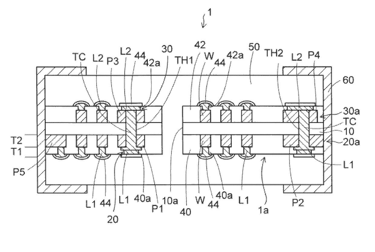
[0053]Hereinafter, an exemplary embodiment will be described with reference to the accompanying drawings.

[0054]Before describing the exemplary embodiment, preliminary matters that are bases of the present invention are first described.

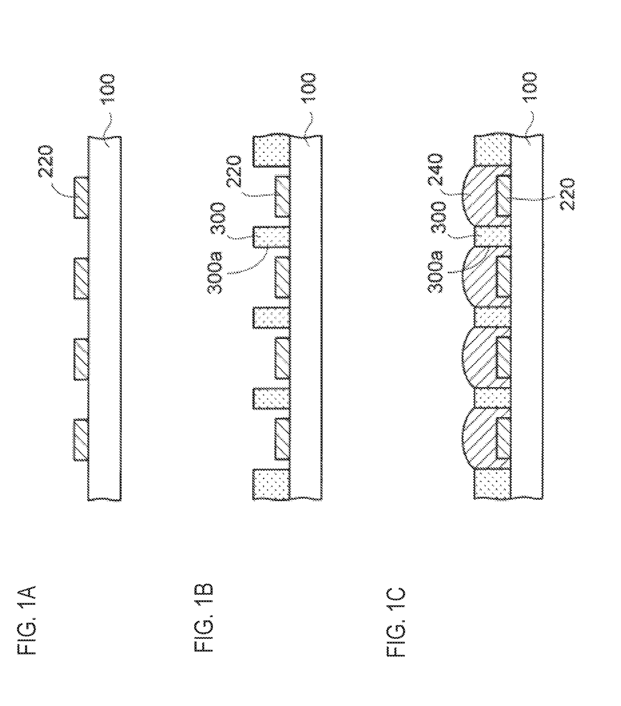
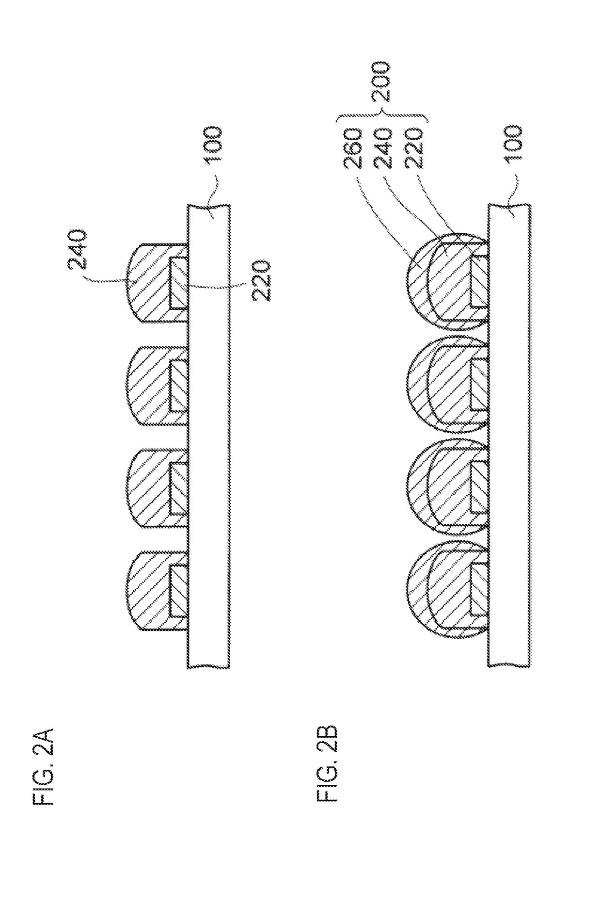
[0055]FIGS. 1A to 2B illustrate a method of forming a conductor pattern layer of an inductor device in accordance with the preliminary matters. The descriptions of the preliminary matters relate to personal investigation contents of the inventors, and include technology contents that are not a well-known technology.

[0056]In a method of forming a conductor pattern layer of an inductor device in accordance with the preliminary matters, as shown in FIG. 1A, a copper layer is first formed on a substrate 100 by plating, and the copper layer is patterned to form a base copper layer pattern 220. The base copper layer pattern 220 is formed as a thin film having a thickness of about 2 μm to 5 μm.

[0057]Then, as shown in FIG. 1B, a pattern of a resist layer 300 h...


PUM


Abstract

An inductor device includes a resin film, a first base conductor layer formed on one surface of the resin film and having a first pad, a second base conductor layer formed on the other surface of the resin film and having a second pad, a through-hole penetrating from the first pad to the second pad, a through conductor filled in the through-hole and provided to connect the first pad and the second pad each other, a first insulating layer formed on the one surface of the resin film and having an opening arranged on the first base conductor layer, and a first conductor part formed on the first base conductor layer in the opening of the first insulating layer. A first conductor pattern layer includes the first base conductor layer and the first conductor part. The first conductor pattern layer has a convex sectional shape.

Description

CROSS-REFERENCE TO RELATED APPLICATION[0001]The present application claims priority from Japanese Patent Application No. 2017-016469 filed on Feb. 1, 2017, the entire content of which is incorporated herein by reference.BACKGROUNDTechnical Field[0002]The present invention relates to an inductor device.Related Art[0003]In the related art, an inductor device that is used for a high frequency circuit of an electronic device and the like has been known. As a structure of the inductor device, a winding type inductor device having an electric wire wound thereto, a planar type inductor device having a spiral coil conductor formed on a plane, and the like have been known.[0004]Patent Document 1: JP-A-2005-210010[0005]Patent Document 2: JP-A-2015-32625[0006]Patent Document 3: JP-A-2015-37179[0007]Patent Document 4: JP-A-2016-9862[0008]As described later in paragraphs of preliminary matters, in a method of forming a conductor pattern layer of an inductor device, a base copper layer pattern of...

Claims


Application Information

Patent Timeline
IPC IPC(8): H01F27/28H01F27/32
CPCH01F27/2852H01F27/2828H01F27/32H01F27/2804H01F2027/2809H01F17/0006H01F27/28H01F27/323H01F41/042H01F41/122H01F17/0013H01F27/29H01F41/046
Inventor NAKANISHI, TSUKASASATO, KIYOKAZUHOSHINO, OSAMU
Owner SHINKO ELECTRIC IND CO LTD
Why Eureka
Try Eureka