Processing method of wafer

a processing method and technology of wafers, applied in the direction of basic electric elements, electrical apparatus, semiconductor devices, etc., can solve the problems of whisker-shaped burrs in the adhesive layer, clogging of the cutting blade, etc., and achieve the effect of convenient disposal

Active Publication Date: 2018-08-09
DISCO CORP
View PDF70 Cites 5 Cited by
  • Summary
  • Abstract
  • Description
  • Claims
  • Application Information

AI Technical Summary

Benefits of technology

[0007]According to the processing method of a wafer in accordance with the present invention, even if the chip size of the singulated chips is as small as 5 mm square or smaller, for example, the occurrence of die shift can be prevented and the die bonding layers can be easily disposed. Furthermore, according to the present invention, the liquid die bonding agent is applied on the back surface and the die bonding layers are disposed at least after the cut grooves are formed in the wafer. Thus, the occurrence of clogging in the cutting blade and generation of a burr or the like in the die bonding layers can be prevented.

Problems solved by technology

However, in the above-described method of Japanese Patent Laid-open No. 2000-182995, there is a problem that clogging occurs in the cutting blade and a whisker-shaped burr is generated in the adhesive layer.

Method used


Image

  • Processing method of wafer
  • Processing method of wafer
  • Processing method of wafer

Examples


Embodiment Construction

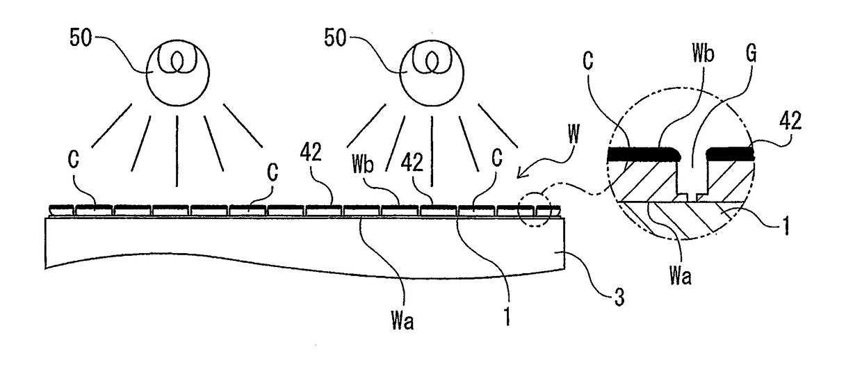
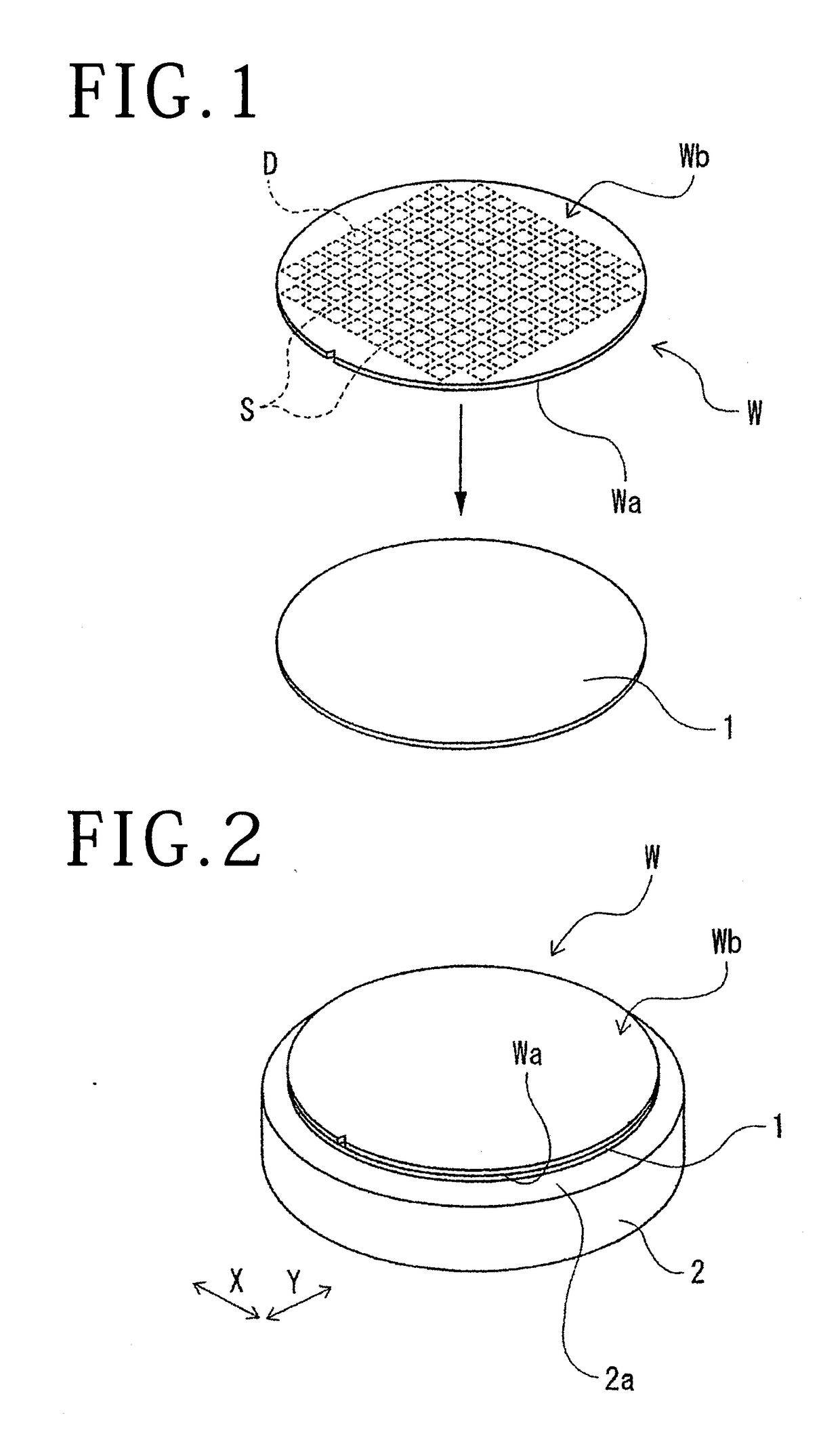
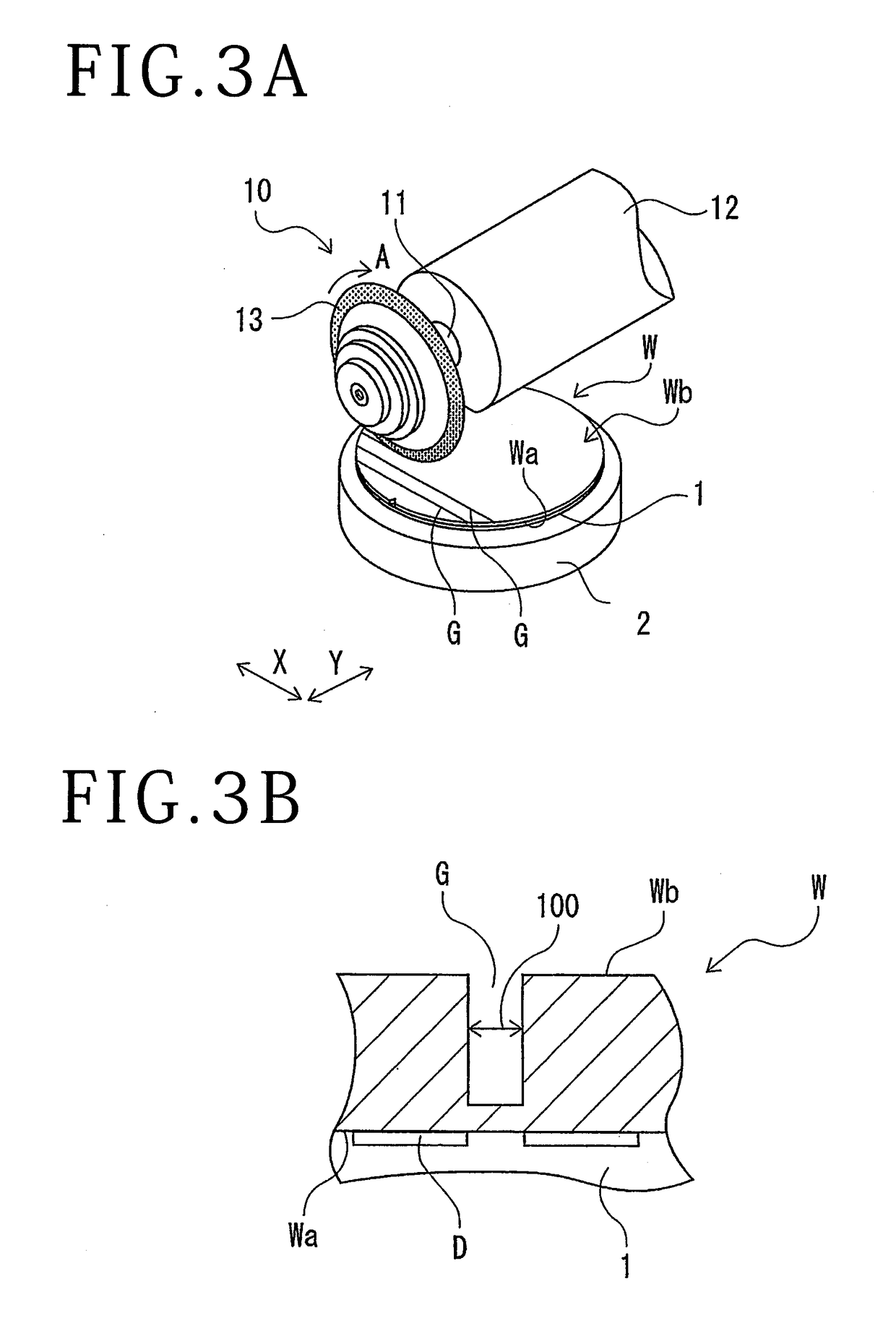
[0016]A wafer W shown in FIG. 1 is one example of a workpiece having a substrate with a circular plate shape and has a front surface Wa on which a device D is formed in each of the respective regions marked out by plural streets S formed in a lattice manner. A back surface Wb on the opposite side to the front surface Wa of the wafer W is a processing-target surface that is subjected to cutting processing by a cutting blade and is irradiated with a laser beam, for example. In the following, a processing method of a wafer for dividing the wafer W into individual chips will be described.

(1) Front Surface Protective Member Disposing Step

[0017]As shown in FIG. 1, a front surface protective member 1 is disposed on the front surface Wa of the wafer W. The front surface protective member 1 has at least a size with substantially the same diameter as the wafer W. When the whole of the front surface Wa of the wafer W is covered by the front surface protective member 1, each device D is protect...


PUM


Abstract

A processing method of a wafer includes a cut groove forming step of carrying out cutting with a cutting blade along streets from the back surface of the wafer to form cut grooves, a wafer dividing step of irradiating the wafer with a laser beam along the cut grooves and dividing the wafer into individual chips after the cut groove forming step is carried out, and a die bonding layer disposing step of applying a liquid die bonding agent on the back surface of the wafer and curing it to form the chips on which die bonding layers are formed on the back surface. According to the processing method of the present invention, the occurrence of clogging in the cutting blade and generation of a burr or the like in the die bonding layers can be prevented.

Description

BACKGROUND OF THE INVENTIONField of the Invention[0001]The present invention relates to a processing method of a wafer for dividing the wafer into individual chips.Description of the Related Art[0002]A wafer on which devices such as integrated circuits (ICs) and large-scale integrated circuits (LSIs) are marked out by planned dividing lines in a lattice manner and are formed on a surface thereof is divided into individual chips having the devices by dividing along the planned dividing lines. In order to mount the individually-divided chips on a metal frame or board (die bonding), chips on which an adhesive layer such as an adhesive film referred to as die attach film (DAF), for example, is formed have been widely employed.[0003]In order to keep chips from being dispersed after a wafer is divided, for example, there is the following method. Specifically, a tape in which an adhesive layer like the above-described one is disposed is adhered to the back surface of the wafer in advance b...

Claims


Application Information

Patent Timeline
Patent Type & Authority Applications(United States)
IPC IPC(8): H01L21/78H01L21/683H01L21/304H01L21/268H01L21/67
CPCH01L21/78H01L21/6838H01L21/3043H01L21/268H01L21/67092H01L21/6836H01L2221/68327H01L21/67115H01L2221/6834
Inventor SUGIYA, TETSUKAZULAN, HEIDI
Owner DISCO CORP
Why Eureka
Try Eureka