Method for determining abnormal equipment in semiconductor manufacturing system and program product

a semiconductor manufacturing system and equipment technology, applied in the field of semiconductor manufacturing techniques, can solve the problems of reducing the yield rate, unable to determine and look for potentially problematic tools in an efficient manner, and the amount of manufacturing history including the tools used and the processing steps, so as to reduce the yield rate, accurately find out, and improve the performance of problematic tools.

Active Publication Date: 2018-08-23
UNITED MICROELECTRONICS CORP
View PDF0 Cites 0 Cited by
  • Summary
  • Abstract
  • Description
  • Claims
  • Application Information

AI Technical Summary

Benefits of technology

[0024]Based on the above, the invention takes an effect of tool stack run count into consideration, so as to make the performance of a problematic to

Problems solved by technology

When the performance of the tool is not as desired, the yield rate may decrease.
However, the amount of data of the manufacturing history including the tools used and the processing steps carrie

Method used


Image

  • Method for determining abnormal equipment in semiconductor manufacturing system and program product
  • Method for determining abnormal equipment in semiconductor manufacturing system and program product
  • Method for determining abnormal equipment in semiconductor manufacturing system and program product

Examples


Embodiment Construction

[0030]Reference will now be made in detail to the present preferred embodiments of the invention, examples of which are illustrated in the accompanying drawings. Wherever possible, the same reference numbers are used in the drawings and the description to refer to the same or like parts.

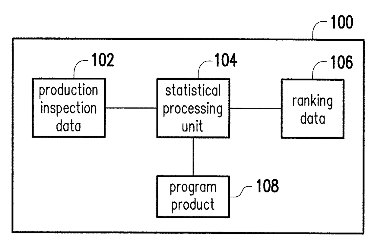
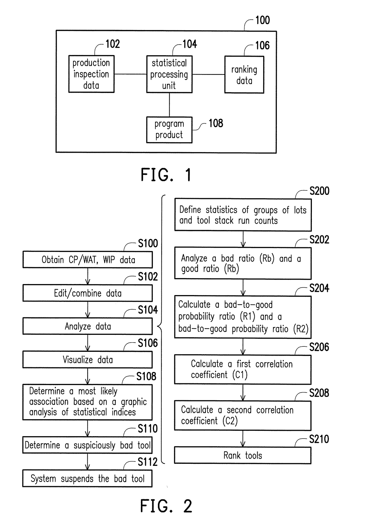
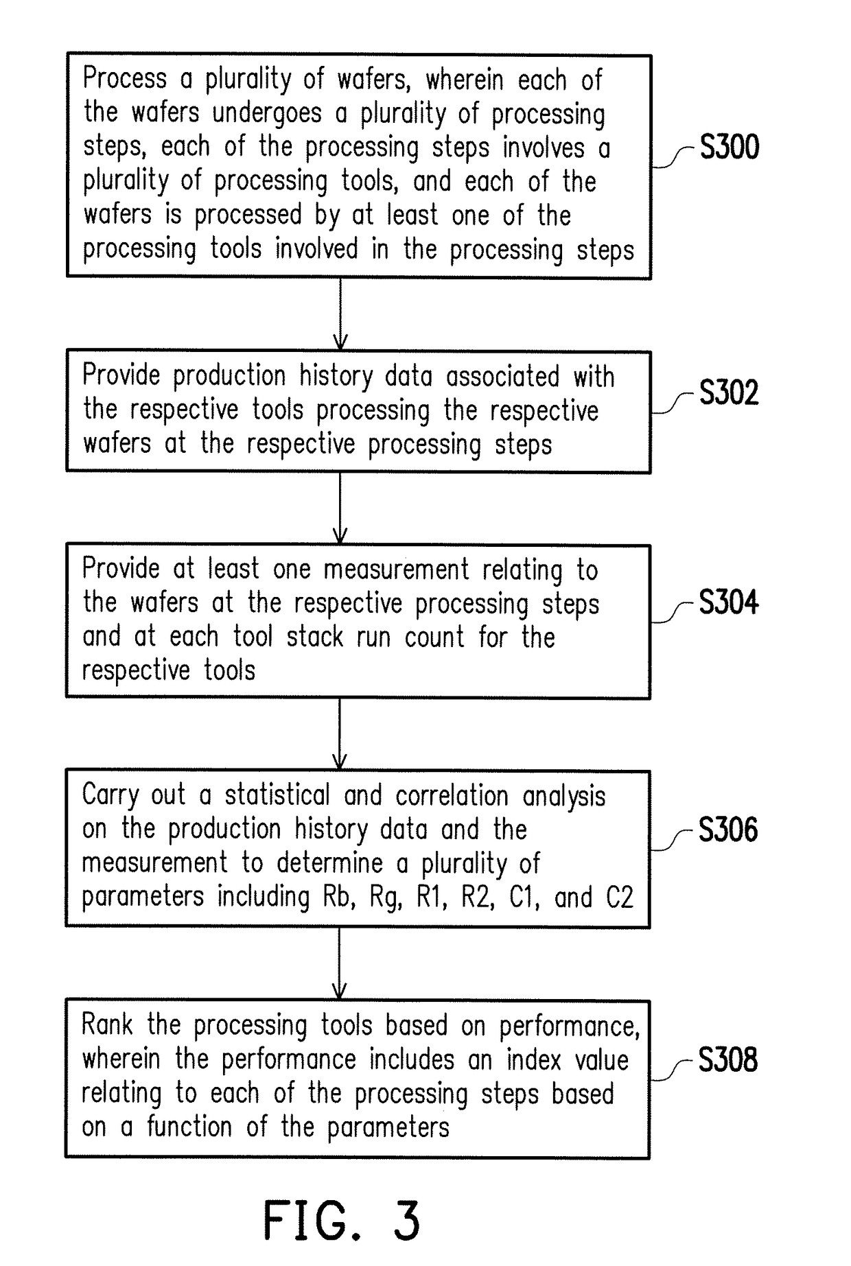
[0031]The invention relates to a method for determining abnormal equipment in a semiconductor manufacturing system and a program product. In the invention, a statistical analysis based on the data of the manufacturing history and the measurement data of the products are carried out systematically. In addition, a plurality of statistical parameters of a plurality of tools is considered, and a correlation analysis is systematically conducted. Then, based on an objective analysis on the performance of tools, the tools are ranked for subsequent decision making based on the chances of causing a decrease in yield rate.

[0032]In the following, some embodiments are provided to describe the invention, but the ...


PUM


Abstract

A method for determining abnormal equipment in semiconductor manufacturing system includes processing wafers. A measurement data relating to wafers at respective processing steps and at each tool stack run count for respective tools is provided. The method also includes performing statistical and correlation analysis on the production history data and the measurement data to determine multiple parameters including bad ratio (Rb) and good ratio (Rg) for each tool. A first bad-to-good probability ratio (R1) for each tool is obtained by dividing Rb by Rg at the tool stack run count. A second bad-to-good probability ratio (R2) of each tool is an overall probability ratio of Rb to Rg of each tool. A first correlation coefficient (C1) is provided for the measurement data corresponding to the tool stack run count. A second correlation coefficient (C2) is provided for the first bad-to-good probability ratio (R1) corresponding to the tool stack run count.

Description

CROSS-REFERENCE TO RELATED APPLICATION[0001]This application claims the priority benefit of Taiwan application serial no. 106105298, filed on Feb. 17, 2017. The entirety of the above-mentioned patent application is hereby incorporated by reference herein and made a part of this specification.BACKGROUND OF THE INVENTION1. Field of the Invention[0002]The invention relates to a semiconductor manufacturing technique, and particularly relates to a method for determining abnormal equipment in a semiconductor manufacturing system and a program product.2. Description of Related Art[0003]When being manufactured, semiconductor products are normally arranged in lots in order for mass production. Each of the lots includes a plurality of wafers for forming semiconductor devices as desired on the wafers. Eventually, a plurality of chips that are not yet packaged are manufactured. Manufacturing of the wafers involves a plurality of processing steps. In each of the steps, a plurality of tools (also...

Claims


Application Information

Patent Timeline
IPC IPC(8): G05B19/418G06F17/18
CPCG05B19/4184G05B2219/45032G05B2219/32191G06F17/18G07C3/14Y02P90/02
Inventor CHEN, LIU-LIANDU, XIAN-FENGZHANG, GUO-HAI
Owner UNITED MICROELECTRONICS CORP
Why Eureka
Try Eureka