Photovoltaic device, photovoltaic cell, and photovoltaic module

Inactive Publication Date: 2018-08-30
NANOBIT TECH
View PDF9 Cites 2 Cited by
  • Summary
  • Abstract
  • Description
  • Claims
  • Application Information

AI Technical Summary

Benefits of technology

[0019]In summary, each of the photovoltaic module, the photovoltaic cell, and the photovoltaic device of the present disclosure is different from the conventional structure (e.g., the structure of the conventional photovoltaic m

Problems solved by technology

The initial drawbacks in the development of photovoltaic cell are the low photoelectric conversion efficiency and the high cost, accordingly, organic photovoltaic cell by using polymer materials draw the industrial and academic domai

Method used


Image

  • Photovoltaic device, photovoltaic cell, and photovoltaic module
  • Photovoltaic device, photovoltaic cell, and photovoltaic module
  • Photovoltaic device, photovoltaic cell, and photovoltaic module

Examples


Example

First Embodiment

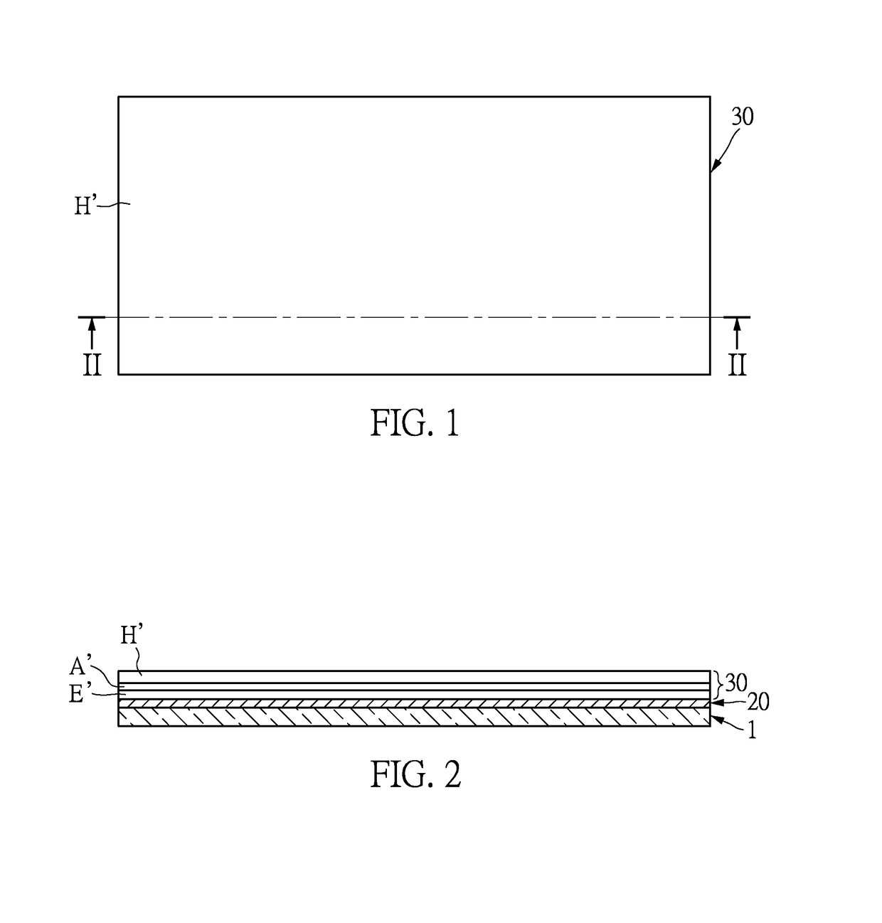
[0035]Reference is made to FIGS. 1 to 12, which illustrate a first embodiment of the present disclosure. The present embodiment discloses a photovoltaic cell 100. The following description first addresses a method for manufacturing the photovoltaic cell 100 in order to clearly describe the structure of the photovoltaic cell 100. The method of the present embodiment includes steps S110 to S150, but the manufacturing method of the photovoltaic cell 100 is not limited thereto.

[0036]Reference is made to FIGS. 1 and 2, which illustrate step S110. A conductive layer 20 and a photovoltaic layer 30 are sequentially stacked on a substrate 1, that is to say, the conductive layer 20 is sandwiched between the conductive layer 20 and the substrate 1. The photovoltaic layer 30 in the present embodiment is a multi-layer structure including an electron transferring layer E′, an active layer A′ stacked on the electron transferring layer E′, and an electronic hole transferring layer H...

Example

Second Embodiment

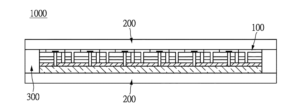
[0058]Reference is made to FIG. 13, which illustrates a second embodiment of the present disclosure. The present embodiment discloses a photovoltaic device 1000 including the photovoltaic cell 100 of the first embodiment, two protective layers 200, and a package compound 300. The photovoltaic cell 100 has been described in the first embodiment, so that the present embodiment will not describe the structure features of the photovoltaic cell 100 again.

[0059]Moreover, the two protective layers 200 are respectively disposed on two opposite sides of the photovoltaic cell 100 (i.e., the top side and the bottom side of the photovoltaic cell 100 as shown in FIG. 13). The package compound 300 is formed to connect the two protective layers 200 and is arranged around the photovoltaic cell 100, such that the photovoltaic cell 100 can be arranged in an enclosed space defined by the package compound 300 and the two protective layers 200.

[0060]Specifically, the package compound 30...


PUM


Abstract

A photovoltaic cell of the present disclosure includes a substrate, a plurality of conductive sheets mutually intervening disposed on the substrate and forming a first matrix arrangement, and a plurality of photovoltaic units mutually intervening disposed on the conductive sheets and forming a second matrix arrangement different from the first matrix arrangement. Moreover, any two adjacent rows of the second matrix arrangement of the photovoltaic units are separated from each other. In each row of the photovoltaic units, an electrical connection of any two adjacent photovoltaic units is established by being connected to one of the conductive sheets. Accordingly, the structure of the photovoltaic cell of the present disclosure can be massively manufactured.

Description

BACKGROUND OF THE INVENTION1. Field of the Invention[0001]The present disclosure relates to a solar battery; in particular, to a photovoltaic device, a photovoltaic cell, and a photovoltaic module.2. Description of Related Art[0002]Solar energy is an inexhaustible and renewable energy in nature, and solar energy obtained from a photovoltaic cell does not produce any pollution, so that solar energy is friendly to the environment as compared to fossil fuels, and the development of photovoltaic cell is important in renewable energy. The initial drawbacks in the development of photovoltaic cell are the low photoelectric conversion efficiency and the high cost, accordingly, organic photovoltaic cell by using polymer materials draw the industrial and academic domains' attention because of the properties such as lower manufacturing cost, lighter material and flexible. However, the structure of conventional photovoltaic cell is too complicated, which results in the difficulty for mass produ...

Claims


Application Information

Patent Timeline
IPC IPC(8): H01L31/05H01L31/02H01L31/049
CPCH01L31/0508H01L31/02008H01L31/049H01L31/0512Y02E10/50H01L31/0465H10K39/10
Inventor CHANG, YU-YANGDING, DING-KUOLIU, SHIOU-MINGHUANG, SUNG-CHIENCHO, CHING-KAI
Owner NANOBIT TECH
Why Eureka
Try Eureka