Surface light-emitting laser

a surface light-emitting laser and nitride-based technology, applied in semiconductor lasers, laser details, electrical devices, etc., can solve the problems of no region available for formation, large difficulty in accurately aligning the two optical axes, optical elements, etc., to accurately determine the position of the light output surface. , the effect of accurate determination

Active Publication Date: 2018-08-30
SONY CORP
View PDF5 Cites 0 Cited by
  • Summary
  • Abstract
  • Description
  • Claims
  • Application Information

AI Technical Summary

Benefits of technology

[0008]In the half-surface-emitting laser according to the embodiment of the technology, the nitride semiconductor layer is provided between the second multi-layer film reflecting mirror and the light output surface. This allows a top surface of the nitride semiconductor layer, or a top surface of some sort of layer provided on the nitride semiconductor layer to serve as the light output surface of the laser element section, which makes it possible to accurately determine the position of the light output surface in the thickness direction by adjusting a thickness of the nitride semiconductor layer, for example. Further, it is possible to provide the optical elements such as the lens and connection terminals of the optical fiber on the top surface o

Problems solved by technology

However, the accurate alignment of both of the optical axes has great difficulty.
This is because, in the nitride-based surface-emitting laser, a bare multi-layer film reflecting mirror is typically formed on a surface exposed by removing a substrate in a manufacturing process, and therefore there is no region available for formation of the above-described optical elements.
Further, it is also very difficult to provide the light output surface of the nitride-based surface-emitting

Method used


Image

  • Surface light-emitting laser
  • Surface light-emitting laser
  • Surface light-emitting laser

Examples


first embodiment

1. First Embodiment

Configuration

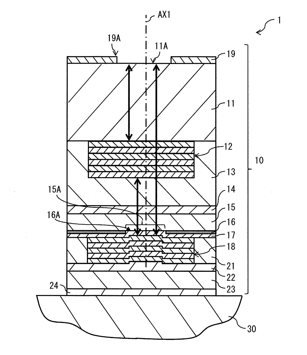
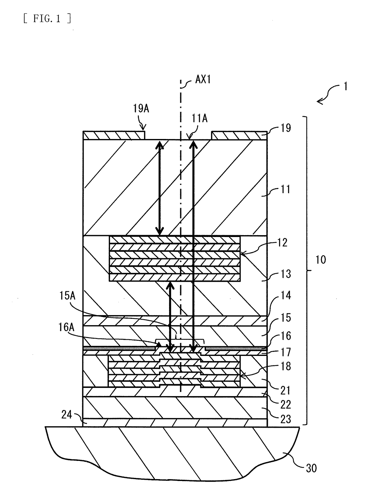
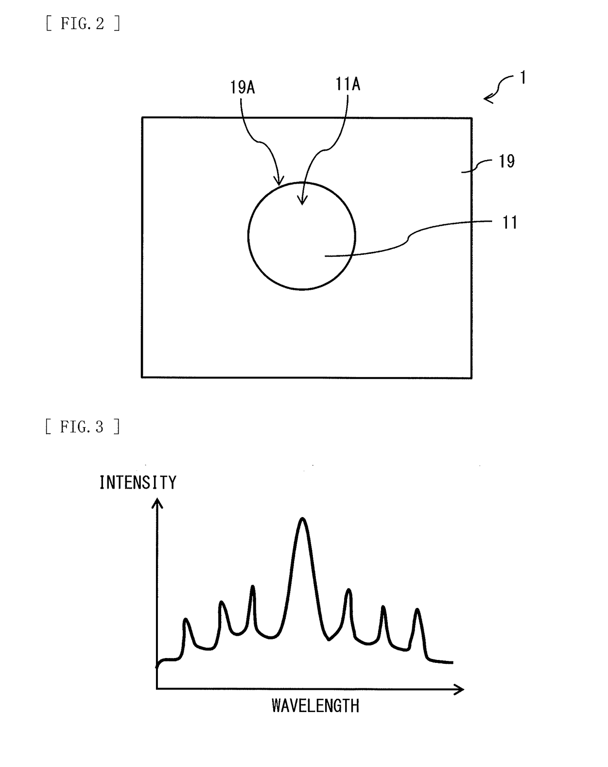
[0062]FIG. 1 illustrates an example of a cross-sectional configuration of a surface-emitting laser 1 according to a first embodiment of the technology. FIG. 2 illustrates an example of a top-side configuration of the surface-emitting laser 1. FIG. 3 illustrates an example of intensity distribution of light to be outputted from a light output surface 11A on a top surface of the surface-emitting laser 1. It is to be noted that FIGS. 1 to 3 are represented schematically, and dimensions and shapes illustrated therein are different from actual dimensions and shapes. In explanation of a configuration of the surface-emitting laser 1, an “upper side” refers to side of the light output surface 11A, and a “lower side” refers to side of a sub-mount section 30 to be described later.

[0063]For example, as illustrated in FIG. 1, the surface-emitting laser 1 includes a laser element section 10 and the sub-mount section 30. In the surface-emitting laser 1, the laser e...

modification example a

[0090]In the above-described embodiment, the multi-layer film reflecting mirror 12 is a dielectric multi-layer film reflecting mirror; however, the multi-layer film reflecting mirror 12 may be a semiconductor multi-layer film reflecting mirror that is formed through the epitaxial growth, as illustrated in FIG. 5, for example. FIG. 5 illustrates a modification example of a cross-sectional configuration of the surface-emitting laser 1 according to the above-described embodiment.

[0091]In the present modification example, the multi-layer film reflecting mirror 12 is a nitride-based semiconductor multi-layer film reflecting mirror that functions as the DBR. A conductivity type of the semiconductor multi-layer film reflecting mirror configuring the multi-layer film reflecting mirror 12 is equivalent to a conductivity type of the semiconductor layer 11. The multi-layer film reflecting mirror 12 is configured in such a manner that two or more kinds of nitride semiconductor layers made of ni...

modification example b

[0093]In the above-described embodiment and modification example A, the top surface of the semiconductor layer 11 is a flat surface; however, a convex mesa portion 11B may be provided on the top surface of the semiconductor layer 11, as illustrated in FIGS. 6 and 7, for example. FIG. 6 illustrates a modification example of a cross-sectional configuration of the surface-emitting laser 1 according to the above-described embodiment. FIG. 7 illustrates a modification example of a cross-sectional configuration of the surface-emitting laser 1 according to the modification example A.

[0094]A top surface of the mesa portion 11B serves as the light output surface 11A, and the electrode layer 19 is provided at a region corresponding to a base of the mesa portion 11B. In the present modification example, in a manufacturing process, after the top surfaces of the semiconductor layers 11 and 41 are formed, the mesa portion 11B is formed at a position corresponding to the light output surface 11A o...


PUM


Abstract

A surface-emitting laser according to one embodiment of the technology includes a laser element section that includes a first multi-layer film reflecting mirror, a first semiconductor layer of a first conductivity type, an active layer, a second semiconductor layer of a second conductivity type, a second multi-layer film reflecting mirror, a nitride semiconductor layer of the second conductivity type, and a light output surface in this order. The laser element section further includes an electrode that injects a current into the active layer.

Description

TECHNICAL FIELD[0001]The technology relates to a nitride-based surface-emitting laser that outputs light in a stacking direction.BACKGROUND ART[0002]In recent years, development of a nitride-based surface-emitting laser has been carried out (for example, see PTLs 1 and 2).CITATION LISTPatent literature[0003]PTL 1: Japanese Unexamined Patent Application Publication No. 2015-35541[0004]PTL 2: Japanese Unexamined Patent Application Publication No. 2015-35542SUMMARY OF THE INVENTION[0005]Meanwhile, to collimate light from a laser, or couple light from each of arrayed lasers, it is necessary to provide optical elements including, for example, a lens and connection terminals of an optical fiber on an output surface of the laser. In providing the above-described optical elements on a light output surface of a nitride-based surface-emitting laser, accurate alignment of an optical axis of the above-described optical elements with an optical axis of the surface-emitting laser allows expected ...

Claims


Application Information

Patent Timeline
IPC IPC(8): H01S5/187H01S5/183H01S5/34H01S5/026
CPCH01S5/18311H01S5/187H01S5/18388H01S5/34H01S5/026H01S5/34333H01S5/18305H01S5/18308H01S5/18341H01S5/18358H01S5/18327H01S5/18333H01S5/18369H01S5/04254H01S5/142H01S5/0215H01S5/1092H01S5/183H01S5/343
Inventor IZUMI, SHOICHIROHAMAGUCHI, TATSUSHIFUTAGAWA, NORIYUKIKURAMOTO, MASARU
Owner SONY CORP
Why Eureka
Try Eureka