
Electronic package and method for manufacturing the same

a technology of electronic packaging and manufacturing methods, applied in the field of packaging techniques, can solve the problems of poor production yield and reliability, reduce production yield, shut down in the manufacturing process, etc., and achieve the effect of balancing the stress of the packaging layer, reducing the overall structure of the electronic package, and smooth manufacturing process

Active Publication Date: 2018-09-06
SILICONWARE PRECISION IND CO LTD
View PDF5 Cites 4 Cited by
  • Summary
  • Abstract
  • Description
  • Claims
  • Application Information

AI Technical Summary

Benefits of technology

This patent is about a way to make electronic packages that have less warping and are more reliable. The method involves adding a layer that balance stress on the back of the package layer, which reduces warping and ensures a smooth manufacturing process. By preventing warping, the method also prevents damage to the electrical connections and increases the yield of reliable products.

Problems solved by technology

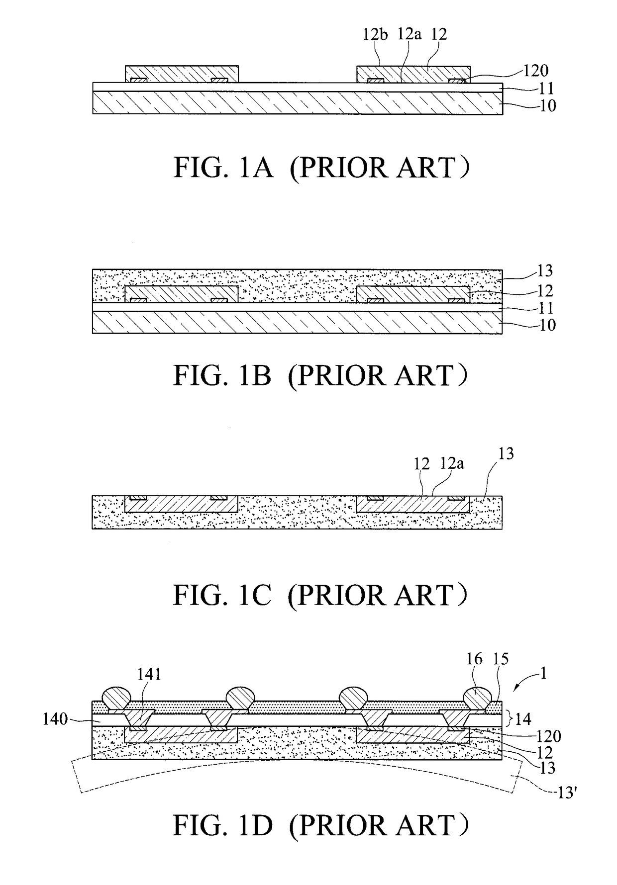
However, in the conventional method for manufacturing a chip scale package, since the encapsulant 13 and the dielectric layer 140 of the circuit structure 14 have quite different coefficients of thermal expansion (CTEs), CTE mismatch occurs, which creates various issues.
Moreover, a large degree of warpage will degrade the reliability of the electrical connections between the semiconductor elements 12 and the circuit layer 141 of the circuit structure 14, resulting in poor production yield and reliability.
Furthermore, warpage may cause fragmentation of the semiconductor elements 12, lowering the production yield.
In addition, large degree of warpage may cause shut down in the manufacturing process of the chip scale package 1, or even affects the reliability of subsequent products.
For example, the chip scale package 1 cannot be placed in the entry of a machine, causing problems associated with the management and manipulation of the machine and hinderance in the production output.

Method used


Image

  • Electronic package and method for manufacturing the same
  • Electronic package and method for manufacturing the same
  • Electronic package and method for manufacturing the same

Examples


Embodiment Construction

[0030]The disclosure is described by the following specific embodiments. Those with ordinary skills in the arts can readily understand other advantages and functions of the disclosure after reading the disclosure of this specification. The present disclosure may also be practiced or applied with other different implementations. Based on different contexts and applications, the various details in this specification can be modified and changed without departing from the spirit of the present disclosure.

[0031]It should be noted that the structures, ratios, sizes shown in the drawings appended to this specification are to be construed in conjunction with the disclosure of this specification in order to facilitate understanding of those skilled in the art. They are not meant, in any ways, to limit the implementations of the disclosure, and therefore have no substantial technical meaning. Without affecting the effects created and objectives achieved by the disclosure, any modifications, c...


PUM


Abstract

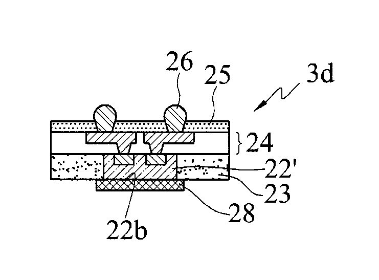
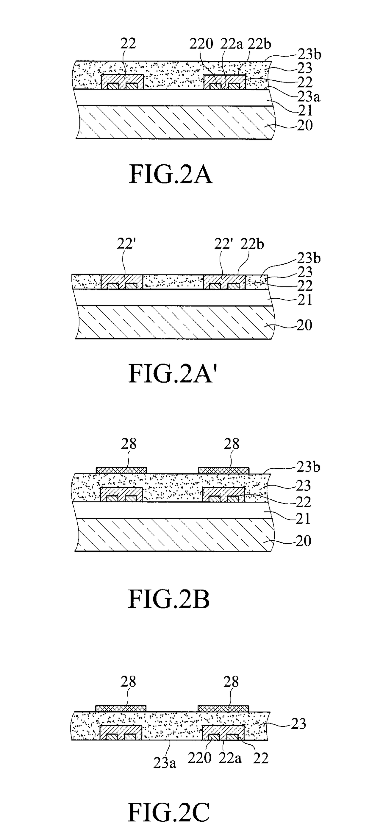
The disclosure provides an electronic package and a method of manufacturing the same. The method is characterized by encapsulating an electronic component with a packaging layer and forming on an upper surface of the packaging layer a circuit structure that is electrically connected to the electronic component; and forming a stress-balancing layer on a portion of the lower surface of the packaging layer to balance the stress exerted on the upper and lower surfaces of the packaging layer, thereby reducing the overall package warpage and facilitating the manufacturing process.

Description

BACKGROUNDTechnical Field[0001]The disclosure is related to packaging techniques, and, more particularly, to an electronic package and a method for manufacturing the same.Description of Related Art[0002]With recent development in electronic industry, electronic products have become more multifunctional and having higher performance. In order to satisfy the packaging demands for miniaturized semiconductor packages, chip scale packaging (CSP) technique has been developed, which is characterized in that a chip scale package only has a size equal to or slighter bigger than that of the chip.[0003]Referring to FIGS. 1A to 1D, schematic cross-sectional views illustrating a conventional method for manufacturing a chip scale package 1 are shown.[0004]As shown in FIG. 1A, a thermal release tape 11 is formed on a carrier 10.[0005]Next, a plurality of semiconductor elements 12 are disposed on the thermal release tape 11. Each of the semiconductor elements 12 has an active surface 12a and a non-...

Claims


Application Information

Patent Timeline
Patent Type & Authority Applications(United States)
IPC IPC(8): H01L23/31H01L23/00H01L21/56H01L21/78
CPCH01L23/3114H01L24/03H01L23/3135H01L21/561H01L21/568H01L21/78H01L24/96H01L2224/0231H01L2224/0237H01L2224/12105H01L2224/13024H01L2924/3511H01L24/13H01L24/05H01L23/562H01L21/56H01L23/31H01L24/26H01L23/16H01L23/3128H01L24/97H01L2224/04105H01L2924/19041H01L2924/19042H01L2924/19043H01L2924/19105H01L2224/18H01L24/19H01L24/20H01L2924/00014H01L2224/05599H01L2924/00012H01L2924/00
Inventor LAI, CHIEH-LUNGCHEN, CHENG-YILU, CHUN-HUNGYEH, MAO-HUA
Owner SILICONWARE PRECISION IND CO LTD
Learn More