Display device, brightness defect correction method for display device, and brightness defect correction device for display device

a display device and brightness defect technology, applied in semiconductor devices, instruments, optics, etc., can solve the problems of difficult to maintain the display quality in the overall display device, common electrodes broken by irradiation, thermal energy adversely affecting other circuits, etc., to suppress the occurrence of luminance defects in the display device, and suppress the occurrence of luminance defects.

Active Publication Date: 2018-09-13
PANASONIC INTELLECTUAL PROPERTY CORP OF AMERICA
View PDF3 Cites 2 Cited by
  • Summary
  • Abstract
  • Description
  • Claims
  • Application Information

AI Technical Summary

Benefits of technology

[0025]The present invention can suppress the occurrence of a luminance defect in the display device.
[0026]According to the present invention, the dimmer including the dimming regions is formed in the display device, thereby suppressing a deterioration of display quality (luminance defect). The display quality is deteriorated because polarization disturbed by a foreign matter trapped in the display device interferes with control on the amount of display light of the display device (the amount of light transmitted from a backlight).

Problems solved by technology

In the method of Japanese Patent Laid-Open No. 2009-080163, however, the common electrode is broken by irradiation with a laser beam.
This may disadvantageously scatter an electrode material during breakage or cause thermal energy adversely affecting other circuits.
Thus, even if display quality reduced by a luminance defect can be improved, it is difficult to maintain the display quality in the overall display device.

Method used


Image

  • Display device, brightness defect correction method for display device, and brightness defect correction device for display device
  • Display device, brightness defect correction method for display device, and brightness defect correction device for display device
  • Display device, brightness defect correction method for display device, and brightness defect correction device for display device

Examples


Embodiment Construction

[0043]An embodiment of the present invention will be described below with reference to the accompanying drawings.

[0044]In the following embodiment, a liquid crystal display will be discussed as an example. The display device of the present invention is not limited a liquid crystal display. For example, an organic electroluminescent display device may be used.

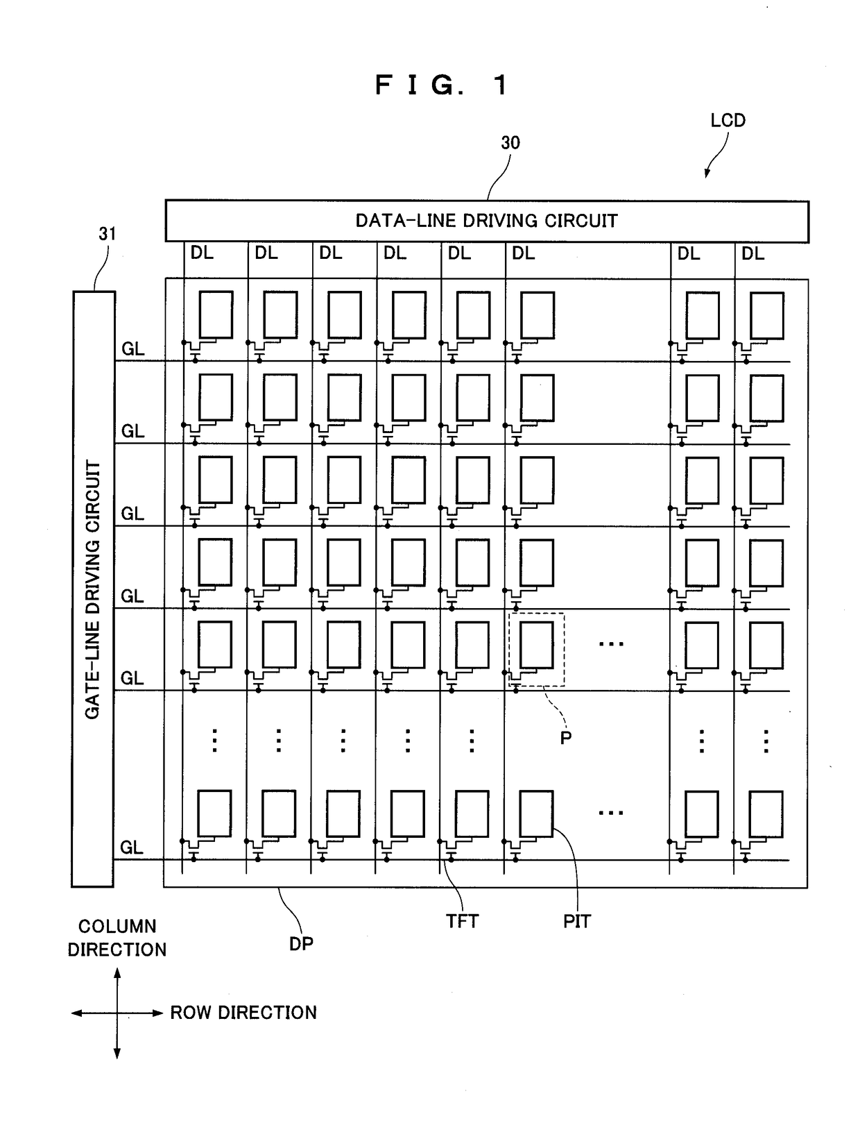
[0045]FIG. 1 is a plan view showing the overall configuration of a liquid crystal display according to the present embodiment.

[0046]A liquid crystal display LCD includes a display panel DP that displays an image, driving circuits (a data-line driving circuit 30, a gate-line driving circuit 31) that drive the display panel DP, a control circuit (not shown) that controls the driving circuits, and a backlight device 37 (FIG. 3) that backlights the display panel DP.

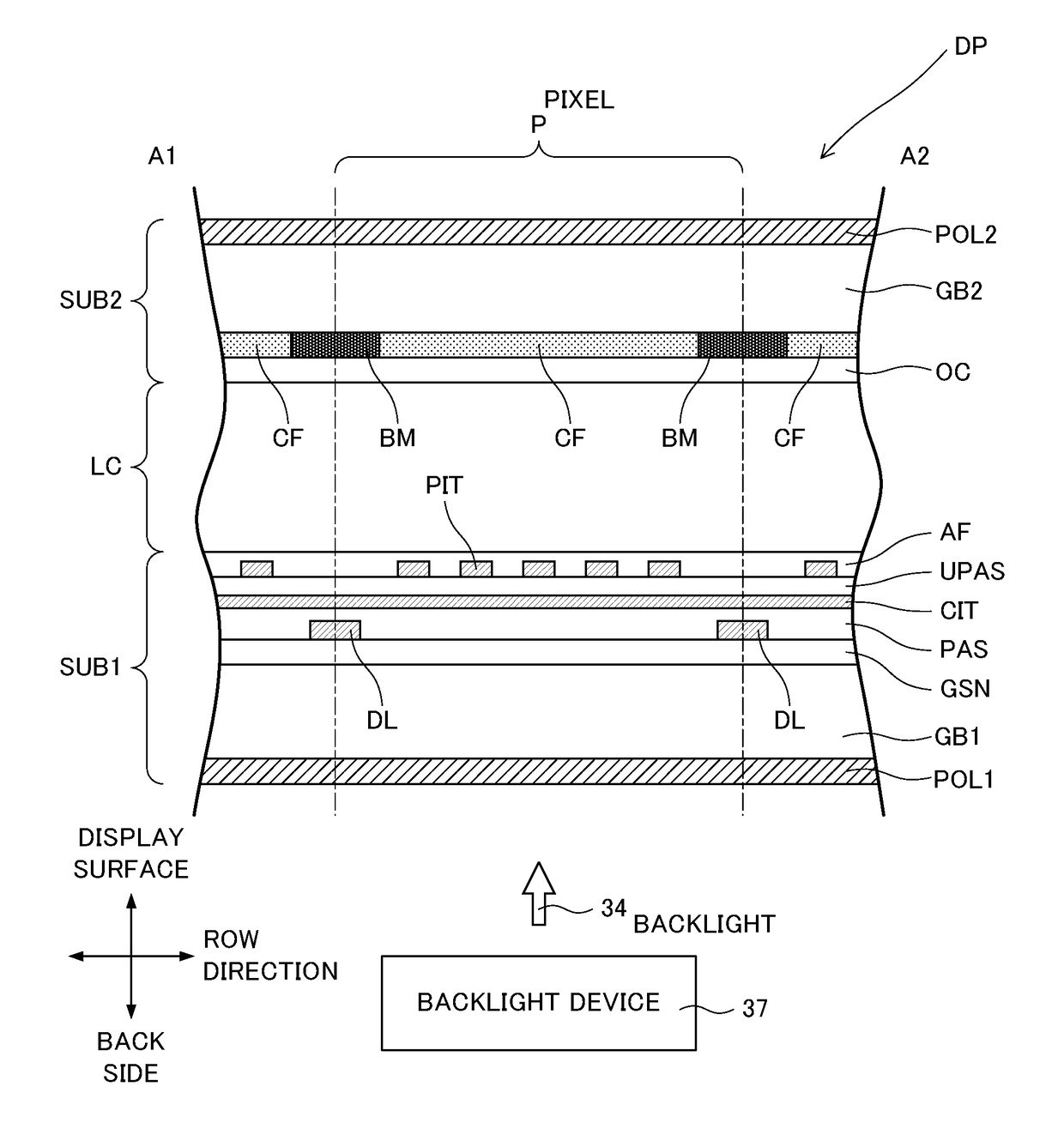
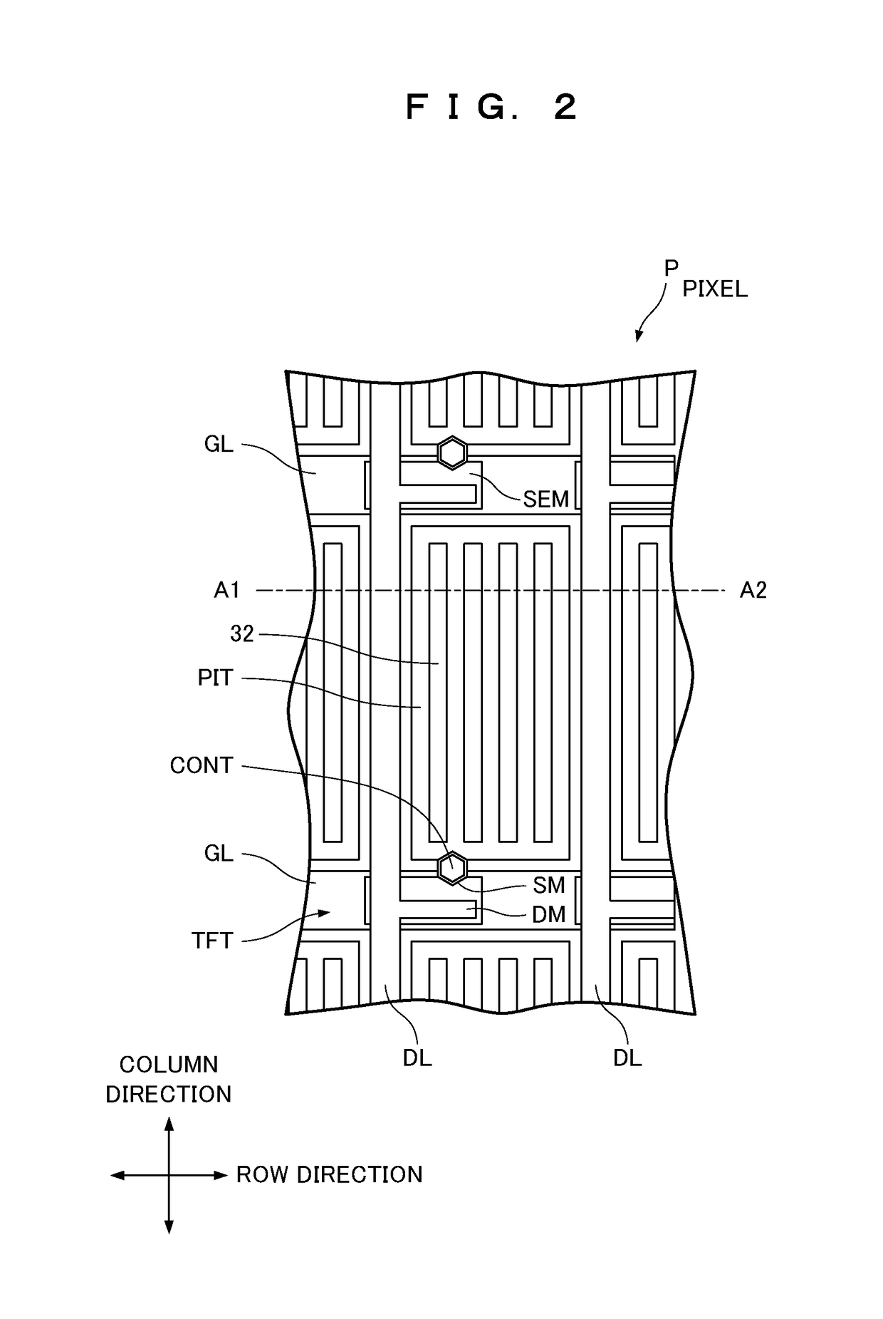
[0047]FIG. 2 is a plan view showing the configuration of a part of the display panel DP. FIG. 3 is a cross-sectional view taken along line A1-A2 of FIG. 2. FIGS. 2 and 3 ...


PUM

PropertyMeasurementUnit
wavelengthaaaaaaaaaa
luminanceaaaaaaaaaa
transmittanceaaaaaaaaaa

Abstract

For suppressing a deterioration of display quality due to a luminance defect, a display device, a method of correcting a luminance defect and a luminance defect corrector are provided. The display device includes a first substrate (SUB1) having gate lines (GL), data lines (DL), pixel electrodes (PIT), and a common electrode (CIT) on a first glass substrate (GB1), and a second substrate (SUB2) having a plurality of optically transparent parts (CF) and a light shield part (BM) on a second glass substrate (GB2). The first or second glass substrate (GB1) or (GB2) contains a dimmer (10) including a plurality of dimming regions (20) that reduce the transmission of light. The dimmer (10) is formed to be superimposed on a trapped foreign matter (33) in plan view. This reduces the transmission of light from the luminance defect to suppress a deterioration of display quality.

Description

FIELD OF THE INVENTION[0001]The present invention relates to a display device, a method of correcting a luminance defect, and a luminance defect corrector.BACKGROUND OF THE INVENTION[0002]Display devices include, for example, a liquid crystal display that applies an electric field generated between a pixel electrode and a common electrode to a liquid crystal layer, which is interposed between a pair of substrates, so as to drive a liquid crystal. This can display an image with an adjusted amount of light passing through a region between the pixel electrode and the common electrode.[0003]In the related art, for example, it is known that a liquid crystal display has a so-called luminance defect (may be called a pixel defect), that is, a pixel having a higher display luminance than a desired luminance. A luminance defect is caused by, for example, a foreign matter trapped between a pair of substrates in the manufacturing process of a liquid crystal display. Such a foreign matter distur...

Claims


Application Information

Patent Timeline
Patent Type & Authority Applications(United States)
IPC IPC(8): G09G3/36G02F1/1335G02F1/133G02F1/1368H01L27/12
CPCG09G3/36G02F1/133514G02F1/133512G02F1/133611G02F1/13306G02F1/1368H01L27/124G02F2201/121G02F2201/123G09G2320/0233G02F1/1309G02F2201/508G09G3/006G09G2330/08G09G2330/10G02F1/136259
Inventor MORI, MASAHIROMORI, SHIGEYUKITANAKA, TAKAONAKAMURA, KAZUYA
Owner PANASONIC INTELLECTUAL PROPERTY CORP OF AMERICA
Why Eureka
Try Eureka