
Methods of forming and operating semiconductor devices including dummy chips

a technology of semiconductor devices and dummy chips, applied in semiconductor devices, semiconductor/solid-state device details, electrical devices, etc., can solve the problems of increased packaging warpage, high cost of tsv interposers, and undesirable forming of fowlp products that include tsv interposers, so as to reduce the total amount of molding compound used and alleviate post-molding warpage

Active Publication Date: 2018-11-08
MICRON TECH INC
View PDF0 Cites 7 Cited by
  • Summary
  • Abstract
  • Description
  • Claims
  • Application Information

AI Technical Summary

Benefits of technology

The solution effectively reduces warpage and manufacturing costs by minimizing the amount of molding compound used, enabling successful assembly of fine-pitch RDL processes without the need for costly TSV interposers.

Problems solved by technology

The TSV interposer is costly because fabricating the interposer substrate with TSVs is a complex process.
Thus, forming FOWLP products that include an interposer having a TSV interposer may be undesirable for certain applications.
The thick layer of the molding compound results in increased warping of the packaging due to coefficient of thermal expansion (CTE) mismatch, and the thickness of the packaging.
Warpage can prevent successful assembly of a die-to-wafer stack because of the inability to maintain the coupling of the die and wafer.
Warpage issue is serious, especially in a large-sized wafer, and has raised an obstacle to a wafer-level semiconductor packaging process that requires a fine-pitch RDL process.

Method used


Image

  • Methods of forming and operating semiconductor devices including dummy chips
  • Methods of forming and operating semiconductor devices including dummy chips
  • Methods of forming and operating semiconductor devices including dummy chips

Examples


Embodiment Construction

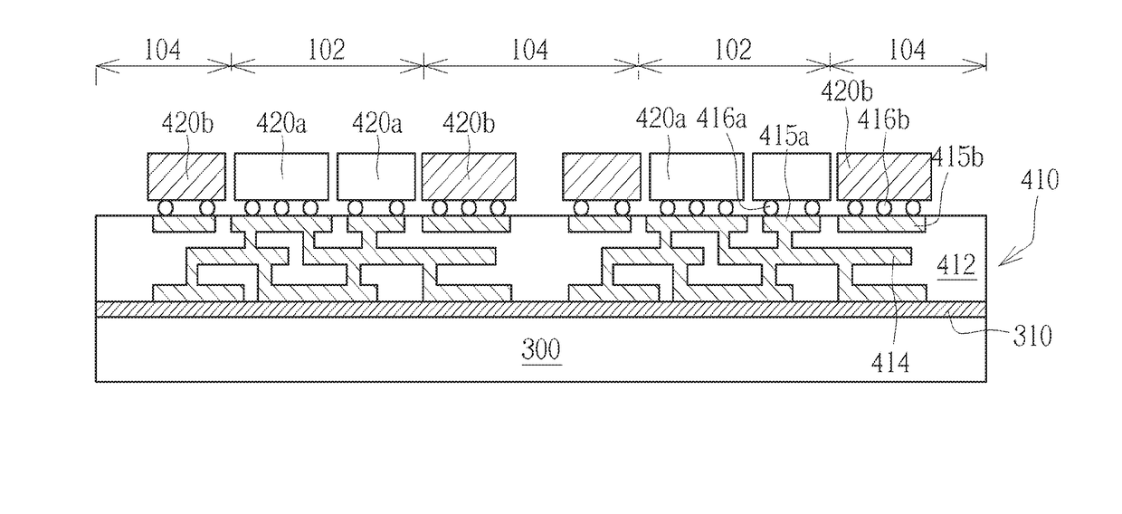
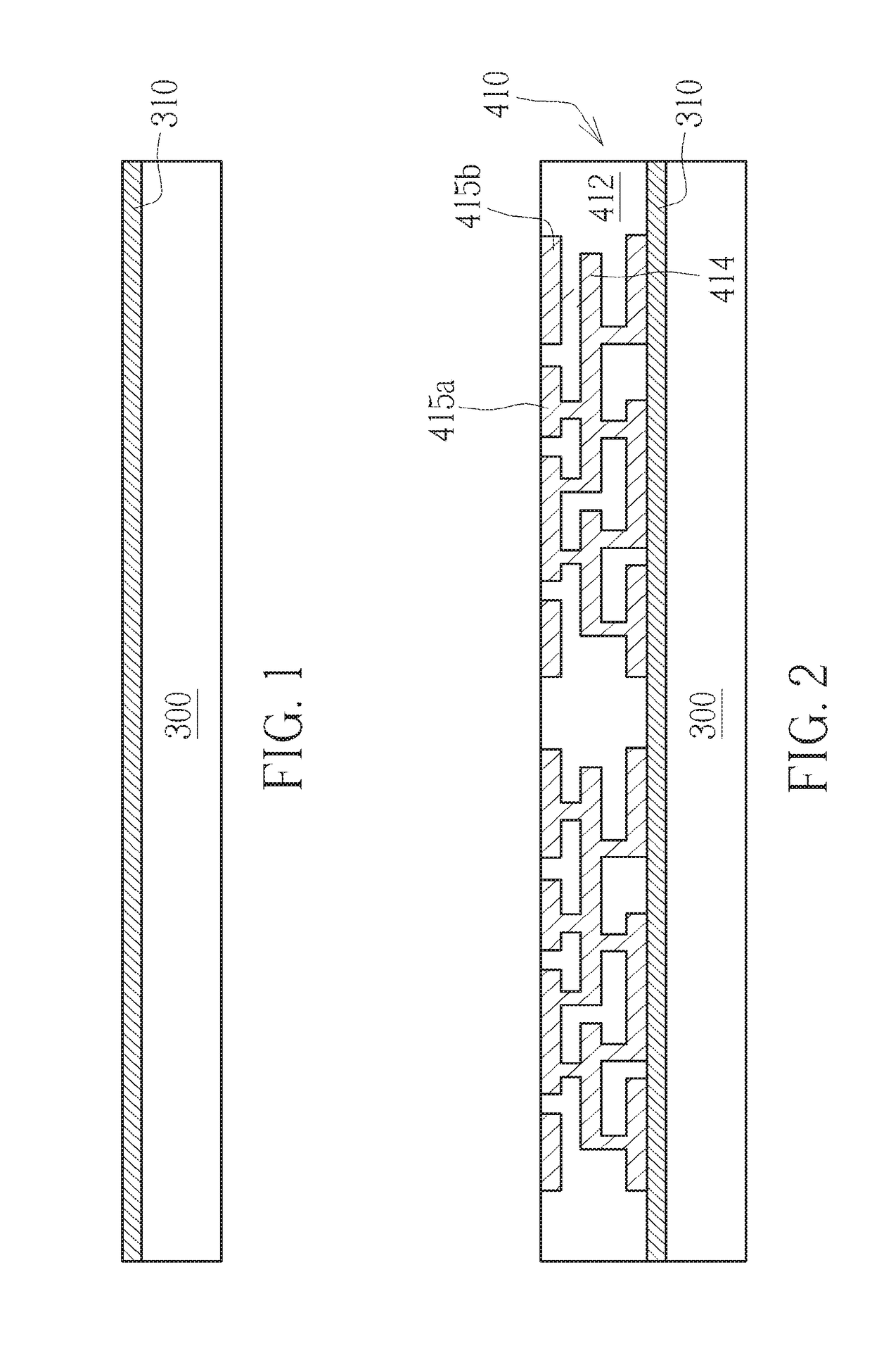
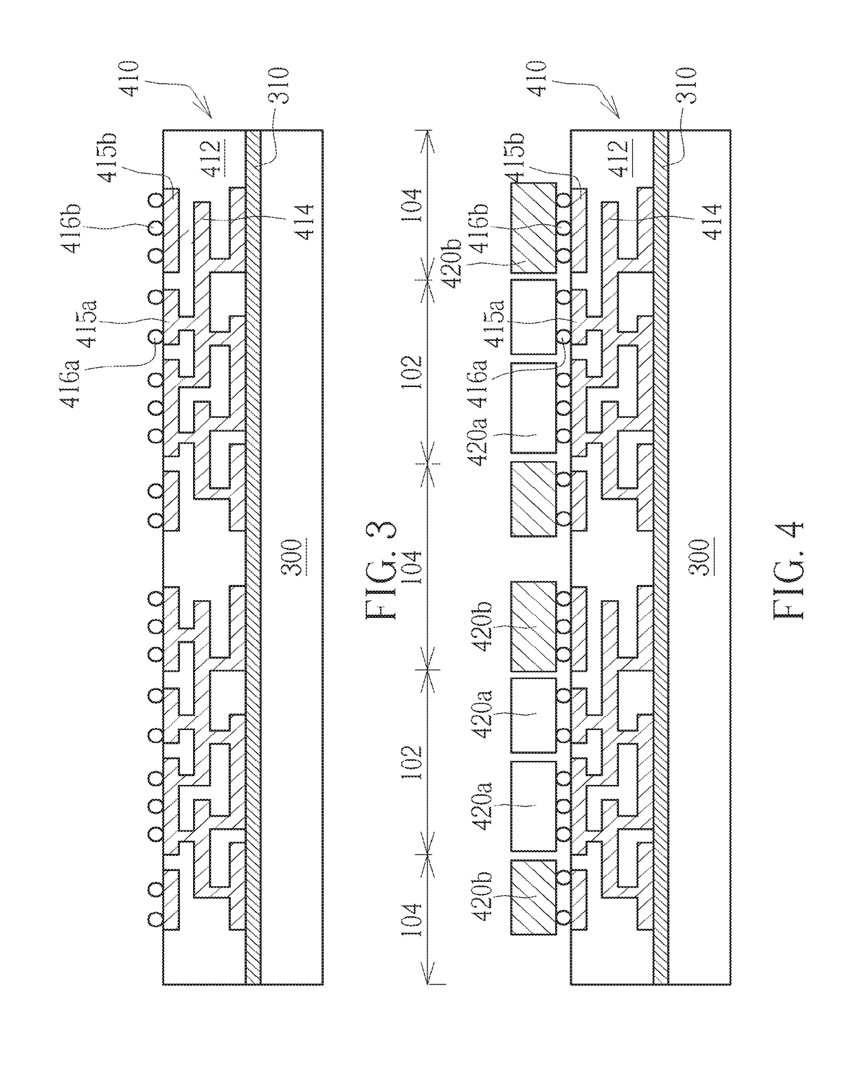
[0018]In the following detailed description of the invention, reference is made to the accompanying drawings, which form a part hereof, and in which is shown, by way of illustration, specific embodiments in which the invention may be practiced. These embodiments are described in sufficient detail to enable those skilled in the art to practice the invention. Other embodiments maybe utilized and structural changes may be made without departing from the scope of the present invention.

[0019]The following detailed description is, therefore, not to be taken in a limiting sense, and the scope of the present invention is defined only by the appended claims, along with the full scope of equivalents to which such claims are entitled.

[0020]One or more implementations of the present invention will now be described with reference to the attached drawings, wherein like reference numerals are used to refer to like elements throughout, and wherein the illustrated structures are not necessarily draw...


PUM


Abstract

A semiconductor device includes an interposer having a first side and a second side opposite to the first side, at least one active chip mounted on the first side within a chip mounting area through a plurality of first bumps, at least one dummy chip mounted on the first side within a peripheral area being adjacent to the chip mounting area, a molding compound disposed on the first side. The molding compound covers the at least one active chip and the at least one dummy chip. A plurality of solder bumps is mounted on the second side.

Description

CROSS-REFERENCE TO RELATED APPLICATION[0001]This application is a continuation of U.S. patent application Ser. No. 14 / 730,231, filed Jun. 3, 2015, pending, the disclosure of which is hereby incorporated herein in its entirety by this reference.TECHNICAL FIELD[0002]The present invention relates generally to the field of semiconductor packaging, and more particularly to a wafer-level package (WLP) with a substrate-less or TSV-less (TSV: Through Substrate Via) interposer and a method for manufacturing the same.BACKGROUND[0003]As known in the art, fan-out wafer-level packaging (FOWLP) is a packaging process in which contacts of a semiconductor die are redistributed over a larger area through a redistribution layer (RDL) that is typically formed on a substrate such as a TSV interposer.[0004]The RDL is typically defined by the addition of metal and dielectric layers onto the surface of the wafer to re-route an Input / Output (I / O) layout into a looser pitch footprint. Such redistribution re...

Claims


Application Information

Patent Timeline
Patent Type & Authority Applications(United States)
IPC IPC(8): H01L23/00H01L25/065H01L21/683H01L21/48H01L21/56H01L23/29H01L23/31H01L23/498H01L25/00
CPCH01L24/81H01L24/02H01L2924/1434H01L2224/92125H01L2224/83005H01L2224/81815H01L2224/81192H01L2224/81005H01L2224/73204H01L2224/32225H01L2224/16227H01L2221/68381H01L2221/68345H01L25/50H01L24/92H01L24/83H01L24/32H01L24/16H01L23/49822H01L23/49816H01L23/3128H01L23/295H01L21/568H01L21/561H01L21/4857H01L25/0655H01L24/97H01L23/562H01L2224/97H01L2924/1432H01L21/6835H01L2924/15192H01L2924/15311H01L2924/18161H01L2924/3511H01L2924/351H01L2224/81H01L2224/83H01L2224/16225H01L2924/00
Inventor SHIH, SHING-YIHSHIH, NENG-TAI
Owner MICRON TECH INC
Features
  • Generate Ideas
  • Intellectual Property
  • Life Sciences
  • Materials
  • Tech Scout
  • Unparalleled Data Quality
  • Higher Quality Content
  • 60% Fewer Hallucinations
Learn More