
Wafer Level Burn-In System

a burn-in system and wafer technology, applied in the direction of semiconductor operation lifetime testing, semiconductor/solid-state device testing/measurement, instruments, etc., can solve the problem of uncut wafer temperature dropping to an undetected low level for testing and curing, and achieve the effect of easy programmability

Active Publication Date: 2018-11-15
DELTA V INSTR INC
View PDF3 Cites 1 Cited by
  • Summary
  • Abstract
  • Description
  • Claims
  • Application Information

AI Technical Summary

Benefits of technology

The patent describes a system for testing semiconductor wafers by using light-up pins and a central processing unit to quickly check if each die is working properly. The system can display test data in real-time and save it for further analysis. The service also includes a feature to vary the test parameters based on the user's needs. The testing process can be customized for each die and can help detect any problems quickly, allowing for timely replacements and avoiding damage to surrounding die. The system is efficient and effective for testing semiconductor wafers.

Problems solved by technology

Without such preheating, and depending to some extent upon ambient temperatures, the lower platen can function as a heat sink and cause the uncut wafer temperature to drop to an undesirably low level for testing and curing.

Method used


Image

  • Wafer Level Burn-In System
  • Wafer Level Burn-In System
  • Wafer Level Burn-In System

Examples


Embodiment Construction

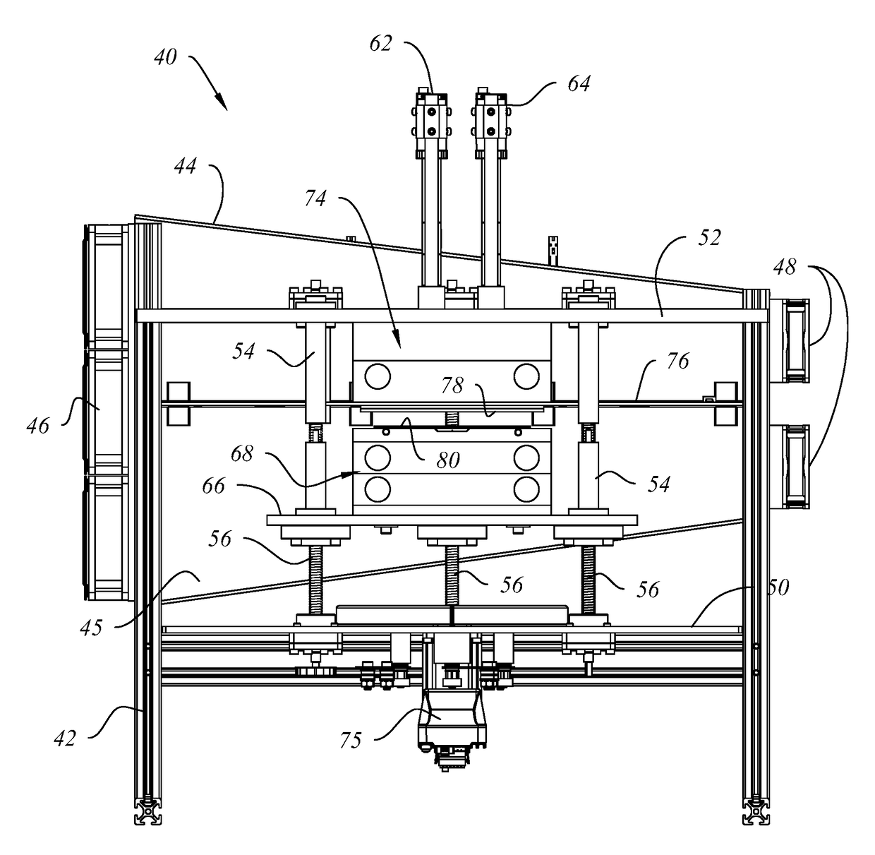
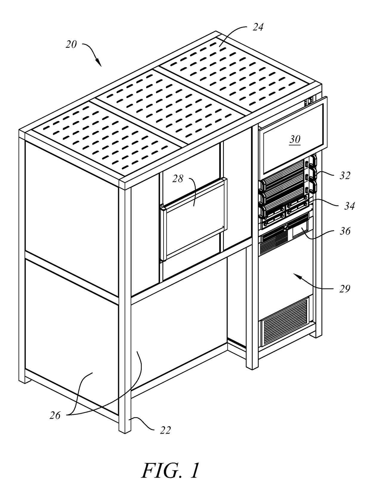
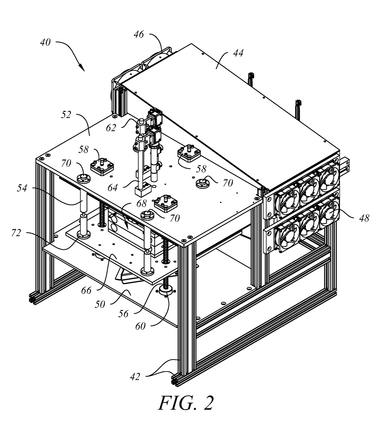
[0035]FIG. 1 discloses one satisfactory embodiment of the apparatus of the invention but for illustrative purposes does not include or show cables, wiring, fittings, connections, flow lines, sensors, transducers, meters or instrumentation for utilities, heaters, chillers, pumps, data transfer, or the like. Referring to FIG. 1, housing 20 comprises frame 22, a plurality of ventilated top panels 24, side panels 26, access door 28, and equipment bay 29. Equipment bay 29 desirably further comprises an electronic equipment rack (not visible) and various ancillary components including without limitation monitor 30, power supplies 32, 34, and back-up power supply 36, and the like. Referring to FIGS. 2-6, wafer burn-in and testing unit 40, which is disposed in a “burn-in bay” inside the proximal portion of housing 20 (FIG. 1), further comprises structural support members 42, upper plenum assembly 44, lower plenum assembly 45, inlet fan assembly 46, outlet plate fans 48, bottom plate 50, upp...


PUM


Abstract

A system for simultaneously burning in, testing and curing all the die on an uncut semiconductor wafer; for establishing electrical connectivity in one-to-one correspondence between each die and a specific current amplifier, for monitoring, displaying, evaluating and recording test parameters in relation to preset parametric limits during a requisite test period; and for shutting down any individual die that exceeds the preset parametric limits. Methods of use and subsystems for raising and lowering a semiconductor wafer in relation to a pin chuck and for controlling wafer temperature by circulating a liquid heat exchange medium through platen assemblies disposed above and below the wafer are also disclosed.

Description

1. FIELD OF THE INVENTION[0001]This invention relates to a device for burning in, testing and curing electronic circuitry that is embodied on small segments, or die, of a semiconductor wafer prior to cutting or dicing the wafers. One aspect of the invention relates to a system, apparatus and method that are capable of simultaneously monitoring and recording test parameters for each of more than 2000 die while also comparing the real-time values to predetermined parametric limits. Another aspect of the invention relates to a die burn-in and test method whereby test data is monitored, displayed and stored at predetermined intervals, and is subsequently recalled, processed, formatted and reported to demonstrate quantitatively the performance and functionality of each die in relation to the predetermined parameters. Another aspect of the invention relates to an apparatus and method of use whereby uncut die on a semiconductor wafer that is determined to be functioning outside predetermin...

Claims


Application Information

Patent Timeline
IPC IPC(8): G01R31/26H01L21/66H01L21/687H01L21/68G01R31/28
CPCG01R31/2642H01L22/14G01R31/2875H01L21/681H01L21/68742G01R31/2862G01R31/2868
Inventor STOREY, ROBERT W.CALDWELL, WILLIAM ROBERTWILSON, CLINT D.PRINCE, GLENN LEECOLLINS, STEPHEN KYLEWALKER, MICHAEL S.CAGE, KERRY F.
Owner DELTA V INSTR INC
Learn More